In
0.53
Ga
0.47
As-In
0.52
Al
0.48
As Multiple Quantum
Well THz photoconductive switches and
In
0.53
Ga
0.47
As-AlAs Asymmetric Spacer Layer
Tunnel (ASPAT) diodes for THz electronics
A thesis submitted to The University of Manchester for the degree of
Doctor of Philosophy
in the Faculty of Science and Engineering
2017
Yuekun Wang
School of Electrical and Electronic Engineering
LIST OF CONTENT
1
LIST OF CONTENT
LIST OF CONTENT ........................................................................................................... 1
LIST OF FIGURES ............................................................................................................. 6
LIST OF TABLES ............................................................................................................. 12
ABSTRACT ........................................................................................................................ 13
DECLARATION ............................................................................................................... 14
COPYRIGHT STATEMENT ........................................................................................... 14
ACKNOWLEDGEMENTS .............................................................................................. 15
PUBLICATIONS ............................................................................................................... 16
CHAPTER 1 : INTRODUCTION .................................................................................... 19
1.1 THz radiation ............................................................................................................. 19
1.2 THz sources ................................................................................................................ 20
1.2.1 Optical approaches .............................................................................................. 20
1.2.2 Electronic approaches .......................................................................................... 22
1.3 THz detectors ............................................................................................................. 23
1.3.1 Direct detection ................................................................................................... 23
1.3.2 Heterodyne detection ........................................................................................... 25
1.3.3 Schottky barrier structures ................................................................................... 26
1.4 Aim and objective ...................................................................................................... 27
1.5 Outline of the thesis ................................................................................................... 28
CHAPTER 2 : BACKGROUND THEORIES ................................................................ 30
2.1 Metal-Semiconductor contacts ................................................................................... 30
2.1.1 Schottky Contacts ................................................................................................ 30
2.1.2 Ohmic contact ...................................................................................................... 34
2.2 THz time domain spectroscopy .................................................................................. 35
2.2.1 THz Pulsed systems ............................................................................................. 36
LIST OF CONTENT
2
2.2.2 THz Continuous Wave (CW) systems ................................................................ 36
2.3 Photoconductive materials ......................................................................................... 37
2.3.1 Low temperature grown GaAs (LT GaAs) .......................................................... 38
2.3.2 Low temperature grown In
0.53
Ga
0.47
As-In
0.52
Al
0.48
As Multiple Quantum Wells
(LT InGaAs-InAlAs MQWs) ....................................................................................... 42
2.4 Electronic devices based on Quantum Mechanical tunnelling .................................. 44
2.4.1 Quantum tunnelling phenomena .......................................................................... 45
2.4.2 Esaki diodes ......................................................................................................... 46
2.4.3 Resonant tunnelling Diode (RTD) ....................................................................... 48
2.4.4 Asymmetric spacer layer tunnelling (ASPAT) diode .......................................... 52
2.4.5 ASPAT detector properties .................................................................................. 54
CHAPTER 3 : EXPERIMENTAL TECHNIQUES ....................................................... 55
3.1 Introduction ................................................................................................................ 55
3.2 Molecular Beam Epitaxy (MBE) growth technique .................................................. 55
3.3 Hall Effect measurements .......................................................................................... 56
3.4 Mid-infrared reflectivity measurements ..................................................................... 59
3.5 Device fabrication ...................................................................................................... 60
3.5.1 Mask design ......................................................................................................... 60
3.5.2 Fabrication process .............................................................................................. 63
3.6 Current-Voltage testing .............................................................................................. 74
3.7 Radio frequency (RF) measurements ......................................................................... 78
CHAPTER 4 : LOW TEMPERATURE GROWN PHOTOCONDUCTIVE
MATERIALS INCORPORATING DISTRIBUTED BRAGG REFLECTORS ......... 79
4.1 Introduction ................................................................................................................ 79
4.2 LT GaAs DBRs structure ........................................................................................... 80
4.2.1 Mid-Infrared reflectivity measurements .............................................................. 83
4.2.2 Hall Effect ........................................................................................................... 84
LIST OF CONTENT
3
4.2.3 Antenna Characterisations ................................................................................... 85
4.3 LT In
0.53
Ga
0.47
As-In
0.52
Al
0.48
As MQWs DBRs structure ........................................... 88
4.3.1 Mid-Infrared reflectivity measurement ............................................................... 90
4.3.2 Hall Effect ........................................................................................................... 91
4.3.3 Antenna Characterisations ................................................................................... 92
4.4 1.55 µm THz spectrometer system ............................................................................ 94
4.4.1 Low temperature grown InGaAs-InAlAs MQWs material ................................. 94
4.4.2 1.55 µm THz spectrometer .................................................................................. 95
4.4.3 Substrate transparency ......................................................................................... 96
4.4.4 THz measurements on other sample objects ....................................................... 99
4.4.5 THz characterisation of biological samples ...................................................... 103
4.5 Summary .................................................................................................................. 105
CHAPTER 5 : In
0.53
Ga
0.47
As-AlAs ASYMMETRIC SPACER LAYER TUNNEL
DIODES ............................................................................................................................ 107
5.1 Introduction .............................................................................................................. 107
5.2 In
0.53
Ga
0.47
As-AlAs asymmetric spacer layer tunnel diodes .................................... 107
5.3 Current-Voltage characterisation ............................................................................. 109
5.3.1 Room temperature DC characterisation ............................................................ 109
5.3.2 Temperature dependency characteristics ........................................................... 114
5.3.3 In
0.53
Ga
0.47
As-AlAs ASPAT diode and Ti/Au SBD .......................................... 116
5.3.4 In
0.53
Ga
0.47
As-AlAs and GaAs-AlAs ASPAT diodes ........................................ 118
5.4 Summary .................................................................................................................. 122
CHAPTER 6 : PHYSICAL MODELLING OF InGaAs-AlAs ASPAT ...................... 124
6.1 Introduction .............................................................................................................. 124
6.2 SILVACO: introduction and specification ............................................................... 124
6.3 Material and model definitions of InGaAs-AlAs ASPAT diode ............................. 125
6.4 ASPAT diode DC Modelling ................................................................................... 129
LIST OF CONTENT
4
6.4.1 Temperature dependence ................................................................................... 134
6.4.2 Temperature dependence simulations of InGaAs-AlAs ASPAT diodes ........... 134
6.5 Material optimisation suggestion ............................................................................. 138
6.6 Summary .................................................................................................................. 141
CHAPTER 7 : DETECTOR CIRCUIT DESIGN USING InGaAs-AlAs ASPAT
DIODES ............................................................................................................................ 142
7.1 Introduction .............................................................................................................. 142
7.2 AC modelling of ASPAT Diode .............................................................................. 142
7.3 De-embedding techniques ........................................................................................ 143
7.4 Comparisons of AC simulation and RF measurement ............................................. 144
7.5 Equivalent Circuit for ASPAT ................................................................................. 148
7.6 Detector circuit design ............................................................................................. 149
7.6.1 ASPAT diode model .......................................................................................... 149
7.6.2 Input power and matching circuit design .......................................................... 151
7.6.3 Detector circuits ................................................................................................. 151
7.7 Summary .................................................................................................................. 159
CHAPTER 8 : CONCLUSIONS AND FUTURE WORK ........................................... 160
8.1 Conclusions .............................................................................................................. 160
8.2 Further Work ............................................................................................................ 163
8.2.1 Photoconductive switches ................................................................................. 163
8.2.2 InGaAs-AlAs ASPAT diode ............................................................................. 163
APPENDIX ....................................................................................................................... 165
Appendix A1: The preparation of Hall Effect samples .................................................. 165
Appendix A2: The fabrication process of photoconductive antennas ........................... 166
Appendix A3: The fabrication process of GaAs-AlAs ASPAT diodes ......................... 168
Appendix A4: The fabrication process of InGaAs-AlAs ASPAT diodes ...................... 174
Appendix B: The instruction of the Rigel 1550 THz spectrometer ............................... 179
LIST OF CONTENT
5
Appendix D: The DC simulation code of InGaAs-AlAs ASPAT diodes ...................... 182
8.2.3 Structure specification ....................................................................................... 183
8.2.4 Material Models Specification .......................................................................... 184
Appendix D: The DC simulation code of InGaAs-AlAs ASPAT diodes ...................... 187
Appendix E: The AC simulation code of InGaAs-AlAs ASPAT diodes ....................... 193
REFERENCES ................................................................................................................. 198
Words count: 47976
LIST OF FIGURES
6
LIST OF FIGURES
Figure 1.1 Schematic of the electromagnetic spectrum indicating that THz radiation is
located between electronics and photonics [2] .................................................................... 19
Figure 1.2 Photoconductive antenna acting as (a) an emitter; (b) a detector ....................... 21
Figure 1.3 Schematic of direct detection [40] ...................................................................... 24
Figure 1.4 Schematic of heterodyne detection [50] ............................................................. 25
Figure 2.1 Schematic band diagram of metal and semiconductor (a) separately and (b) in
contact [63] .......................................................................................................................... 31
Figure 2.2 Energy band diagram of Schottky contact on n-type material under (a) reverse
bias and (b) forward bias [63] .............................................................................................. 32
Figure 2.3 The equivalent circuit of a diode [63] ................................................................ 33
Figure 2.4 Schematic and photo of a waveguide based zero bias detector and (b) RF
performance of a VDI Schottky detector [68] ..................................................................... 34
Figure 2.5 Typical THz TDS system setup [71] .................................................................. 35
Figure 2.6 Equivalent circuit model for a THz photoconductive antenna [82] ................... 37
Figure 2.7 Resistivity and carrier lifetime as functions of anneal temperature, for a LT
GaAs photoconductive antenna [90] .................................................................................... 40
Figure 2.8 (a) Sheet resistivity versus inverse measurement temperature for as grown and
annealed LT GaAs; (b) Hall mobility versus temperature for as grown and annealed LT
GaAs [96] ............................................................................................................................. 41
Figure 2.9 Temporal evolution of transmission change of a homogeneously Be-doped LT
InGaAs-lnAlAs multilayer structure[106] ........................................................................... 44
Figure 2.10 Wave functions showing electron tunnelling through a rectangular barrier [63]
............................................................................................................................................. 46
Figure 2.11 Band diagrams of tunnel diode at (a) thermal equilibrium (zero bias); (b)
forward bias V such that peak current is obtained; (c) forward bias approaching valley
current; (d) forward bias with diffusion current and no tunnelling current; and (e) reverse
bias with increasing tunnelling current [63] ........................................................................ 48
Figure 2.12 Band diagrams of RTDs under different bias conditions (a) Zero bias; (b)
threshold bias; (c) resonant tunnelling through Er; (d) off resonance and (e) the I-V
characteristics of the RTDs [116] ........................................................................................ 50
Figure 2.13 The conduction band profile of ASPAT under different bias .......................... 52
LIST OF FIGURES
7
Figure 2.14 Epitaxial layer profile structures of GaAs-AlAs ASPAT ................................ 53
Figure 2.15 The E-k diagram of (a) GaAs and (b) AlAs [126] ........................................... 54
Figure 3.1 (a) Schematic diagram of a typical MBE system for the growth of In
0.53
Ga
0.47
As
on InP substrate[133] (b) Photo of V100HU MBE system used in this work. ................... 56
Figure 3.2 Schematic of the Hall Effect phenomena ........................................................... 57
Figure 3.3 Van der Pauw geometry Hall Effect sample ...................................................... 58
Figure 3.4 Hall Effect measurements set ups used in this work .......................................... 58
Figure 3.5 Reflectivity measurement system ....................................................................... 59
Figure 3.6 Reflectivity measurement setup ......................................................................... 59
Figure 3.7 Fabrication process flow for (a) design 1; (b) design 2 ...................................... 61
Figure 3.8 Geometry of coplanar waveguide ....................................................................... 61
Figure 3.9 The complete 15×15 mm
2
mask designed using Agilent ADS software (a)
dielectric design (b) air-bridge design ................................................................................. 62
Figure 3.10 Close-up view of a single ASPAT diode with 6 µm×6 µm mesa area (dielectric
layer and air-bridge) ............................................................................................................. 62
Figure 3.11 Picture of MA4 mask aligner system ............................................................... 64
Figure 3.12 Pattern differences generated from the use of positive and negative photoresist
[139] ..................................................................................................................................... 65
Figure 3.13 Sample after spin coating stage ........................................................................ 65
Figure 3.14 Average etching rates for (a) GaAs and (b) InGaAs using Orthophosphoric-
based etchant at different ratios ........................................................................................... 68
Figure 3.15 Cross sectional view of InGaAs device (a) ideal etch (b) practical wet etch ... 69
Figure 3.16 Average etching rates for GaAs using Ammonium Hydroxide-based etchants
............................................................................................................................................. 69
Figure 3.17 Schematic of RIE system ................................................................................. 71
Figure 3.18 Rapid Thermal Annealer used in this work ...................................................... 72
Figure 3.19 Evaporator set-ups (a) Bio Rad and (b) Edwards Auto 306 ............................. 73
Figure 3.20 Lift-off process with the negative photoresist undercut profile ....................... 73
Figure 3.21 Annealing equipment (a) alloying jig and (b) furnace ..................................... 74
Figure 3.22 Pictures of (a) B1500A semiconductor device analyser and (b) Lakeshore
Cryogenic probe station used in this study .......................................................................... 75
Figure 3.23 Four-Point probes TLM measurements set up ................................................. 75
Figure 3.24 Schematic drawing for top-view of TLM structure .......................................... 76
LIST OF FIGURES
8
Figure 3.25 Plot of resistance versus spreading distance in TLM structure ........................ 76
Figure 3.26 Cross section of an ASPAT showing the epi-layers and contacts .................... 77
Figure 3.27 Photo of VNA system set up ............................................................................ 78
Figure 4.1 Physical structures along with the layer thicknesses of (a) XMBE 305 and (b)
XMBE 316 (Both structures were designed to operate at 800 nm wavelength) .................. 81
Figure 4.2 Reflectance as a function of wavelength (GaAs-AlAs DBRs) ........................... 81
Figure 4.3 Comparison of the reflection for 8 pairs of GaAs-AlAs DBRs with theoretical
thicknesses and the optimised thicknesses ........................................................................... 83
Figure 4.4 Normalised reflectivity of XMBE316 with different etching depths ................. 84
Figure 4.5 Photo of Cloverleaf Van der Pauw geometry Hall Effect sample ...................... 85
Figure 4.6 Antenna geometries (a) Aperture and (b) Dipole ............................................... 86
Figure 4.7 (a) THz pulses and (b) normalized Fourier transform power spectrum emitted
from large aperture antenna fabricated on the XMBE316 (LT GaAs with DBR) and
detected by a dipole antenna fabricated on the XMBE305 (LT GaAs) ............................... 87
Figure 4.8 Physical structures along with the layer thicknesses of (a) XMBE 290 and (b)
XMBE 329 (Both structures were designed to operate at 1550 nm) ................................... 89
Figure 4.9 Reflectance as a function of wavelength (GaAs-AlAs DBRs) ........................... 89
Figure 4.10 Normalised reflectivity of XMBE329 with different etching depths ............... 91
Figure 4.11 (a) THz pulses and (b) normalized Fourier transform power spectrum emitted
and detected by dipole antennas made on XMBE329 ......................................................... 93
Figure 4.12 Compact THz photoconductive antenna modules ............................................ 96
Figure 4.15 Rigel 1550 THz spectrometer measurements (a) THz pulses with air reference
and SI InP: Fe wafer in the sample holder (b) comparison of the power spectrums from
both measurements .............................................................................................................. 97
Figure 4.16 Rigel 1550 THz spectrometer measurements (a)THz pulses with air reference
and SI GaAs wafer in the sample holder and (b) comparison of the power spectrums from
both measurements .............................................................................................................. 98
Figure 4.17 Rigel 1550 THz spectrometer measurements: comparison of (a) Field
amplitude spectrums and (b) the power spectrums from paper and air measurements ..... 100
Figure 4.18 Rigel 1550 THz spectrometer measurements: comparison of (a) Field
amplitude spectrums and (b) the power spectrums from paper and air measurements ..... 101
Figure 4.19 Absorption spectrum for ten pieces of paper .................................................. 102
LIST OF FIGURES
9
Figure 4.20 Rigel 1550 THz spectrometer measurements: comparison of (a) Field
amplitude spectrums and (b) the power spectrums from cotton fibre and air measurements
........................................................................................................................................... 103
Figure 4.21 power spectrums from haploid and doubled haploid plants measurements ... 104
Figure 4.22 Rigel 1550 THz spectrometer measurements: comparison of (a) Field
amplitude spectrums (b) the power spectrums from human hand and air ......................... 105
Figure 5.1 Physical structure and band profile along with layers thicknesses of XMBE 326
........................................................................................................................................... 108
Figure 5.2 Schematic conduction band profile of an ASPAT diode under bias
(In
0.53
Ga
0.47
As-AlAs ASPAT in red and GaAs-AlAs in black) ......................................... 109
Figure 5.3 XMBE326 TLM measurements for the top contact after annealing at 280 ˚C for
2 mins. ................................................................................................................................ 109
Figure 5.4 The DC measurement set-up (device size is 30×30 µm
2
) ................................ 110
Figure 5.5 (a) Cross-sectional view of complete undercut area beneath the air bridge and (b)
Top view of the fabricated air bridge device ..................................................................... 111
Figure 5.6 Current densities of XMBE326 ASPAT diodes using baked dielectric bridge 112
Figure 5.7 Current densities of XMBE326 ASPAT diodes using as-designed air-bridge 112
Figure 5.8 Schematic of undercut area of the air-bridge design ........................................ 113
Figure 5.9 Current densities of XMBE326 ASPAT diodes factoring in estimated undercut
........................................................................................................................................... 113
Figure 5.10 Current densities of XMBE326 ASPAT Factoring in optimised undercut .... 114
Figure 5.11 Epitaxial layer profile for XMBE304 (GaAs-AlAs ASPAT) ........................ 115
Figure 5.12 Epitaxial layers for XMBE104 (SBD) ........................................................... 116
Figure 5.13 Temperature dependence of (a) SBD device and (b) InGaAs-AlAs ASPAT
device (100×100 µm
2
) ....................................................................................................... 117
Figure 5.14 Temperature dependence of the current for both SBD and ASPAT for 100×100
µm
2
size devices ................................................................................................................ 118
Figure 5.15 Current densities of XMBE304 ASPAT diodes using dielectric bridge ........ 119
Figure 5.16 Temperature dependence of GaAs-AlAs ASPAT device (100×100 µm
2
) ..... 120
Figure 5.17 Temperature dependence of the current for GaAs-AlAs and InGaAs-AlAs
ASPAT diodes for 100×100 μm
2
size devices ................................................................... 120
Figure 5.18 Calculated current variations for both GaAs-AlAs and InGaAs-AlAs ASPAT
diodes over the entire temperature range ........................................................................... 122
LIST OF FIGURES
10
Figure 6.4 XMBE326 structure and layer profile used in the simulation .......................... 125
Figure 6.5 Band diagram of XMBE326 ASPAT (under zero bias) ................................... 128
Figure 6.6 The conduction band profile for ASPAT under bias from SILVACO Simulation
........................................................................................................................................... 128
Figure 6.7 3D Structure of ASPAT including contacts and semi-insulating substrates .... 129
Figure 6.8 Back-contacted structure (3D Structure) .......................................................... 130
Figure 6.9 Simulated DC characteristic differences between back-contacted and planar
structure ............................................................................................................................. 130
Figure 6.10 Simulated DC characteristics for InGaAs-AlAs ASPAT with different
bandgaps ............................................................................................................................ 132
Figure 6.11 Room Temperature measured vs simulated data of I-V characterisations for
XMBE326 ASPAT diodes with mesa area of 63.2 µm
2
.................................................... 133
Figure 6.12 Room Temperature measured vs simulated data of I-V characterisations for
XMBE326 ASPAT diodes with various mesa sizes .......................................................... 133
Figure 6.13 Measurements and simulations comparisons at 125 K, 225 K and 350 K ..... 137
Figure 6.14 Potential barrier height: simulated results comparison between GaAs-AlAs and
In
0.53
Ga
0.47
As-AlAs ASPAT diodes ................................................................................... 138
Figure 6.15 Second derivative of the InGaAs-AlAs ASPAT diode IV characteristics ..... 139
Figure 6.16 Barrier thickness variations of InGaAs-AlAs ASPAT (4×4 μm²) ................. 140
Figure 6.17 Thicker spacer thickness variation for InGaAs-AlAs ASPAT (4×4 μm²) ..... 141
Figure 7.1 Photographs of the CPW Structures (a) Open and (b) Short ............................ 143
Figure 7.2 Compared S11 parameters in Smith Chart a) ‘Open’ and b) ‘Short’ ............... 144
Figure 7.3 Simulated and Measured Capacitance for GaAs-AlAs and In
0.53
Ga
0.47
As /AlAs
ASPAT Diodes (4×4 μm²) ................................................................................................. 145
Figure 7.4 Simulated Conductance for GaAs-AlAs and In
0.53
Ga
0.47
As-AlAs ASPAT Diodes
(4×4 μm²) ........................................................................................................................... 146
Figure 7.5 (a) ADS Equivalent Circuit for ASPAT diode (4×4 μm²): SILVACO S-
parameter Block incorporating parasitic and (b) Physical Modelling vs. Measurement
Results of the ASPAT diodes ............................................................................................ 147
Figure 7.6 (a) Measured and simulated equivalent circuit and (b) S-parameters for InGaAs-
AlAs ASPAT diode (4×4 μm²) .......................................................................................... 149
Figure 7.7 Measured I-V characteristics of InGaAs-AlAs ASPAT diode (4×4 μm²) and
polynomial model fit. ......................................................................................................... 150
LIST OF FIGURES
11
Figure 7.8 SDD-block empirical model used to represent ASPAT diodes in ADS ......... 150
Figure 7.9 Detector circuit using ASPAT diode nonlinear component ............................. 152
Figure 7.10 Transfer functions of 4×4 μm² InGaAs-AlAs ASPAT diode at 100 GHz ..... 153
Figure 7.11 Voltage sensitivity of 4×4 μm² InGaAs-AlAs ASPAT diode at 100 GHz as a
function of input power ...................................................................................................... 153
Figure 7.12 Voltage sensitivity of 4×4 μm² InGaAs-AlAs ASPAT diode with respect of
input RF frequency (100 GHz) .......................................................................................... 154
Figure 7.13 Transfer functions of 4×4 μm² InGaAs-AlAs ASPAT diode at 240 GHz ..... 155
Figure 7.14 Voltage sensitivity of 4×4 μm² InGaAs-AlAs ASPAT diode at 240 GHz as a
function of input power ...................................................................................................... 155
Figure 7.15 Voltage sensitivity of 4×4 μm² InGaAs-AlAs ASPAT diode with respect of
input RF frequency (240 GHz) .......................................................................................... 156
Figure 7.16 Voltage sensitivity of 4×4 μm² InGaAs-AlAs ASPAT diode with respect of
input RF frequency (350 K) ............................................................................................... 158
LIST OF TABLES
12
LIST OF TABLES
Table 2-1 Mobility of GaAs grown at different temperatures [97] ..................................... 42
Table 2-2 In
0.8
Ga
0.2
As-AlAs RTD with Indium-rich quantum well grown by MBE .......... 49
Table 2-3 Lattice constant and band gap of common III-V binary and ternary
semiconductors [115] ........................................................................................................... 49
Table 3-1 Photoresists with their corresponding spinner setting and developing times ...... 66
Table 4-1 The reflectance of GaAs-AlAs DBRs ................................................................. 82
Table 4-2 Hall Effect measurements of LT GaAs samples ................................................. 85
Table 4-3 The reflectance of GaAs-AlAs DBRs ................................................................. 90
Table 4-4 Hall Effect measurements of In
0.53
Ga
0.47
As-In
0.52
Al
0.48
As samples .................... 92
Table 6-1 Key physical parameters used in SILVACO simulation ................................... 127
Table 6-2 Effective masses of GaAs and In
0.53
Ga
0.47
As at various temperatures .............. 135
Table 6-3 Energy band gaps of AlAs, GaAs and In
0.53
Ga
0.47
As at various temperatures .. 136
Table 7-1 Extracted values for the intrinsic components for 4 × 4 µm² devices at zero bias
........................................................................................................................................... 148
Table 7-2 Comparisons of SBDs and InGaAs-AlAs ASPAT detectors ............................ 157
ABSTRACT
13
ABSTRACT
Thesis Title: In
0.53
Ga
0.47
As-In
0.52
Al
0.48
As Multiple Quantum Well THz photoconductive
switches and In
0.53
Ga
0.47
As-AlAs Asymmetric Spacer Layer Tunnel (ASPAT) diodes for
THz electronics
Name: Yuekun Wang
Degree: Doctor of Philosophy
University: The University of Manchester
Date: 2017
This thesis is concerned with terahertz (THz) technology from both optical and electronic
approaches. On the optical front, the investigation of optimised photoconductive switches
included the characterisation, fabrication and testing of devices which can generate and
detect THz radiation over the frequency range from DC to ~ 2.5 THz. These devices
incorporated semiconductor photoconductors grown under low temperature (LT)
Molecular Beam Epitaxy (MBE) conditions and using distributed Bragg reflectors (DBRs).
The material properties were studied via numerous characterisation techniques which
included Hall Effect and mid infrared reflections. Antenna structures were fabricated on
the surface of the active layers and pulsed/continuous wave (CW) signal absorbed by these
structures (under bias) generates photocurrent. With the help of the DBRs at certain
wavelengths (800 nm and 1550 nm), the absorption coefficient at the corresponding
illumination wavelength increased thus leading to significant increase of the THz output
power while the materials kept the desirable photoconductive material properties such as
high dark resistivity and high electron mobility. The inclusion of DBRs resulted in more
than doubling of the THz peak signals across the entire operating frequency range and
significant improvements in the relative THz power.
For the THz electronic approach, a new type of InP-based Asymmetric Spacer Tunnel
Diode (ASPAT), which can be used for high frequency detection, was studied. The
asymmetric DC characteristics for this novel tunnel diode showed direct compatibility with
high frequency zero-bias detector applications. The devices also showed an extreme
thermal stability (less than 7.8% current change from 77 K to 400 K) as the main carrier
transport mechanism of the ASPAT was tunnelling.
Physical models for this ASPAT diode were developed for both DC (direct current) and
AC (alternating current) simulations using the TCAD software tool SILVACO. The
simulated DC results showed almost perfect matches with measurements across the entire
temperature range from 77 K to 400 K. From RF (radio frequency) measurements, the
intrinsic diode parameters were extracted and compared with measured data. The simulated
zero biased detector circuits operating at 100 GHz and 240 GHz using the new InGaAs-
AlAs ASPAT diode (44 μm
2
) showed comparable voltage sensitivities to state of the art
Schottky barrier diodes (SBDs) detectors but with the added advantage of excellent
thermal stability.
DECLARATION AND COPYRIGHT
14
DECLARATION
No portion of the work referred to in the thesis has been submitted in support of an
application for another degree or qualification of this or any other university or other
institute of learning.
COPYRIGHT STATEMENT
i. The author of this thesis (including any appendices and/or schedules to this thesis) owns
certain copyright or related rights in it (the “Copyright”) and s/he has given The University
of Manchester certain rights to use such Copyright, including for administrative purposes.
ii. Copies of this thesis, either in full or in extracts and whether in hard or electronic copy,
may be made only in accordance with the Copyright, Designs and Patents Act 1998 (as
amended) and regulations issued under it or, where appropriate, in accordance with
licensing agreements which the University has from time to time. This page must form part
of any such copies made.
iii. The ownership of certain Copyright, patents, designs, trademarks and other intellectual
property (the “Intellectual Property”) and any reproductions of copyright works in the
thesis, for example graphs and tables (“Reproductions”), which may be described in this
thesis, may not be owned by the author and may be owned by third parties. Such
Intellectual Property and Reproductions cannot and must not be made available for use
without the prior written permission of the owner(s) of the relevant Intellectual Property
and/or Reproductions.
iv. Further information on the conditions under which disclosure, publication and
commercialisation of this thesis, the Copyright and any Intellectual Property and/or
Reproductions described in it may take place is available in the University IP policy IP
Policy (see http://documents.manchester.ac.uk/DocuInfo.aspx?DocID=487), in any
relevant Thesis restriction declarations deposited in the University Library, The University
Library’s regulations (see http://www.manchester.ac.uk/library/aboutus/regulations) and in
the University’s policy on Presentation of Theses.
ACKNOWLEDGEMENTS
15
ACKNOWLEDGEMENTS
First and foremost, I would like to express my sincere gratitude to my supervisor Prof.
Mohamed Missous for the continuous support of my PhD study and research, for his
patience, motivation, enthusiasm and immense knowledge. His guidance helped me greatly
in my research and during the writing of this thesis.
I extend my thanks to the industrial partners TeTechS Inc and Integrated Compound
Semiconductors Ltd for THz TDS testing and high frequency measurements. Without their
support, this project would not have been possible.
My sincere thanks also go to all my colleagues in the School of Electrical and Electronic
Engineering for the discussions, support and for all the fun we had.
I am also deeply indebted to my family and friends for their love, support and
understanding throughout my life.
Finally, I would like to thank and acknowledge the China Scholarship Council for
financially supporting my study.
PUBLICATIONS
16
PUBLICATIONS
A. JOURNAL PUBLICATIONS
1. Y. Wang, I. Kostakis, D. Saeedkia and M. Missous, “Optimised THz
photoconductive devices based on low-temperature grown III–V compound
semiconductors incorporating distributed Bragg reflectors,” IET Optoelectronics, vol. 11,
no. 2, pp. 53-57, 2017.
2. K. N. Zainul Ariffin, Y. Wang, M. R. R. Abdullah, S. G. Muttlak, Omar S.
Abdulwahid, J. Sexton, Ka Wa Ian, Michael J. Kelly and M. Missous, “Investigations of
Asymmetric Spacer Tunnel Layer (ASPAT) Diodes for High-Frequency Applications,”
Transactions on Electron Devices, accepted.
3. Mundher Al-Shakban, Peter David Matthews, Nicky Savjani, Xiang L Zhong,
Yuekun Wang, Mohamed Missous and Paul O'Brien, “The synthesis and characterization
of Cu2ZnSnS4 thin films from melt reactions using xanthate precursors,” Journal of
Materials Science, accepted.
B. CONFERENCE PAPERS AND PRESENTATIONS
1. Y. Wang, M. Missous, Daniel M. Hailu, Alireza Zandieh, Ehsan Fathi, and
Daryoosh Saeedkia, “Optimized THz photoconductor devices operating at 800 nm and
1550 nm excitation wavelengths”, UK Semiconductors 2014, University of Sheffield, July,
2014
2. Y. Wang, I. Kostakis and M. Missous, D.M. Hailu, A. Zandieh, E. Fathi and D.
Saeedkia, “Advanced LT-InGaAs-InAlAs 1550 nm photoconductive switches for a
portable fiber coupled THz spectrometer”, Photon 2014, Imperial College London,
September, 2014
3. Alireza Zandieh, Daniel Hailu, Ehsan Fathi, Yuekun Wang, Ioannis Kostakis,
Mohamed Missous, Safieddin Safavi-Naeini, and Daryoosh Saeedkia, “A Novel
Photoconductive Antenna With A Band Gap Structure For Terahertz Applications”, 39th
International Conference on Infrared, Millimeter, and Terahertz Waves, the University of
Arizona, September, 2014, IEEE proceedings
PUBLICATIONS
17
4. Yuekun Wang and M. Missous, “Photoconductive antennas for all-fibre
terahertz spectrometer operating at 1550nm telecom wavelength”, Postgraduate Poster
Conference, University of Manchester, February, 2015
5. Yuekun Wang, Mohd Rashid Redza Abdullah and M. Missous, “InGaAs/AlAs
asymmetric space layer tunnel (ASPAT) diodes for THz electronics”, UK Semiconductors
2015, University of Sheffield, July, 2015
6. Yuekun Wang, Mohd Rashid Redza Abdullah, James Sexton and M. Missous,
“Temperature dependence characteristics of In
0.53
Ga
0.47
As/AlAs asymmetric spacer-layer
tunnel (ASPAT) diode detectors”, 8th UK-Europe-China Workshop on mm-waves and
THz Technologies, Cardiff University, September, 2015, IEEE proceedings
7. M.R.R Abdullah, Y. K. Wang, J. Sexton, M. Missous and M. J. Kelly,
“GaAs/AlAs Tunnelling Structure: Temperature Dependence of ASPAT Detectors”, 8th
UK-Europe-China Workshop on mm-waves and THz Technologies, Cardiff University,
September, 2015, IEEE proceedings
8. K.N. Zainul Ariffin, S.G. Muttlak, M. Abdullah, M.R.R. Abdullah, Y. Wang,
and M. Missous, “Asymmetric Spacer Layer Tunnel In
0.18
Ga
0.82
As/AlAs (ASPAT) Diode
using Double Quantum Wells for Dual Functions: Detection and Oscillation”, 8th UK-
Europe-China Workshop on mm-waves and THz Technologies, Cardiff University,
September, 2015, IEEE proceedings
9. Yuekun Wang, Ioannis Kostakis, Daryoosh Saeedkia and Mohamed Missous,
“Optimized THz Devices based on low-temperature grown III-V semiconductor
compounds,” Semiconductor and Integrated Opto-electronics conference: SIOE’2016,
Cardiff University, April, 2016
10. Yuekun Wang, Khairul Nabilah Zainul Ariffin, Kawa Ian and Mohamed
Missous, “Physical Modelling and experimental studies of InGaAs/AlAs Asymmetric
spacer layer tunnel diodes,” UK Semiconductors 2016, University of Sheffield, July, 2016
11. M.R.R Abdullah, Y. Wang, J. Sexton, Kawa Ian and Mohamed Missous,
“Microwave Performance of GaAs-AlAs Asymmetric Spacer Layer Tunnel (ASPAT)
Diodes,” UK Semiconductors 2016, University of Sheffield, July, 2016
PUBLICATIONS
18
12. K.N. Zainul Ariffin, S.G. Muttlak, M. Abdullah, M.R.R. Abdullah, Y. Wang,
and M. Missous, “Experimental and Physical Modelling of Temperature Dependence of a
Double Quantum Well In
0.18
Ga
0.82
As-AlAs ASPAT diode,” UK Semiconductors 2016,
University of Sheffield, July, 2016
13. Yuekun Wang, Khairul Nabilah Zainul Ariffin, Kawa Ian, M.J. Kelly and
Mohamed Missous, “RF performance of In
0.53
Ga
0.47
As/AlAs Asymmetric spacer layer
tunnel diodes,” UK Semiconductors 2017, University of Sheffield, July, 2017
14. K.N. Zainul Ariffin, M.R.R. Abdullah, Y. Wang, S.G. Muttlak, O.S.
Abdulwahid, J. Sexton, and M. Missous, “Asymmetric Spacer Layer Tunnel Diode
(ASPAT), Quantum Structure Design Linked to Current-Voltage Characteristics: A
Physical Simulation Study,” 10th UK-Europe-China Workshop on mm-waves and THz
Technologies, University of Liverpool, September, 2017, IEEE proceedings

CHAPTER 1
19
CHAPTER 1: INTRODUCTION
1.1 THz radiation
THz radiation, also known as submillimetre radiation, encompasses frequencies from about
100 GHz to 10 THz with corresponding wavelength range from 3 mm to 0.3 mm [1]. The
THz region is located between microwaves and far infrared light. The electromagnetic
spectrum highlighting the THz portion is shown Figure 1.1 [2].
Example
industries:
Radio
communications
Radar
Optical
communications
Medical
imaging
kilo mega giga tera peta exa zetta yotta
Frequency (Hz)
1 THz ~ 1 ps ~ 300 μm ~ 4.1 meV
10
0
10
3
10
6
10
9
10
12
10
15
10
18
10
21
10
24
THz
photonics
electronics
microwaves
visible
x-ray
γ-ray
Astrophysics
Figure 1.1 Schematic of the electromagnetic spectrum indicating that THz radiation is
located between electronics and photonics [2]
The many reasons that make THz such an active area of intense research are the facts that
this radiation is highly absorbed by water, is transparent to many opaque materials and can
penetrate deep into many organic materials. These properties make THz technology
particularly suitable for use in chemistry, biology, astrophysics and many other
applications. In addition, unlike X-rays, THz radiation can penetrate deep into organic
materials without any damage since its energy is not high enough to break chemical bonds.
This further makes THz a promising candidate for security and medical applications [3].
Before the 1980s, it was extremely difficult to generate and detect THz radiation.
Thereafter, extensive reports on mode-locked picosecond and sub-picosecond pulsed lasers
made it possible to create short carrier lifetime semiconductor-based switches for THz time
domain spectroscopy including both generation and detection of THz radiation [4]. During
the following decades, a great deal of interest was aimed at developing systems with high
CHAPTER 1
20
output power. Currently, commercial time domain THz systems that with reasonably
priced and improved reliability and performance are available [5], albeit still bulky.
1.2 THz sources
Due to the THz region lying between optics and microwave, the generation of THz
radiation can be established via two different approaches: (i) frequency down conversion
from the optical region and (ii) frequency up conversion from the microwave region using
solid state electronic devices.
1.2.1 Optical approaches
For down conversion from the optical region, a nonlinear crystal with a large second order
susceptibility can be used for THz generation and detection, an example being ZnTe which
is one of the most widely used electro-optic (EO) crystals in THz applications [6]. EO
crystal with large second order nonlinear optical susceptibilities can be used as both
emitters and detectors. The mechanism for this THz generation is based on optical
rectification and the THz radiation energy is obtained from a laser source. In practice, EO
crystals acting as the THz source should be kept thin in order to minimise the velocity
mismatch which is used to avoid destructive interferences [7].
In addition, for down conversion from the optical region, Gas lasers [8] and Quantum
Cascade Lasers (QCL) [9] can be used. Gas lasers are optically pumped with their
operation based on CO
2
lasers which excites gas molecules with the THz frequency of the
molecular lasers being dependent on the spectral line of the gas used. THz QCLs are based
on super-lattice semiconductor materials and the THz radiation is generated by electron
propagating through coupled quantum wells. The first demonstrated THz QCLs emitting at
4.4 THz were reported in 2002 [10]. This frequency was subsequently shifted down to 0.95
THz [11]. The operating frequency of QCLs can be controlled by the quantum well designs.
The main reasons which limit the wide application of THz QCLs are that the systems need
cryogenic cooling and are of limited reliability [12].
Amongst all existing optically excited THz sources, one of the most extensively used
sources is the photoconductive antenna which consists of electrode metals with designed
geometry on the surface of a photoconductive material. The photoconductive switches are
key devices which allow both the reliable generation and detection of broadband THz

CHAPTER 1
21
radiation [13]. Using photoconductive antennas is also the most efficient way for down-
converting optical signal to THz radiation and is widely used in spectroscopy and imaging
applications [14, 15]. The photoconductive switches were first reported in 1970s [16].
They can not only be used as THz emitters but also as receivers.
For emission, a photoconductive antenna needs to be DC biased. Electron-hole pairs can be
created in the femtosecond time scale when an ultrafast laser pulse is shone on the gap of
the antenna. Due to acceleration of the carriers in the electric field originating in the
surface depletion layer of the photoconductor, a THz wave can be radiated (Magnetic-
field-enhanced generation of terahertz radiation in semiconductor surfaces).
The detection process can be treated as the reverse of the generation mechanism. In most
cases, no bias voltage is applied across the electrodes, and the incident THz radiation
induces a voltage across the antenna which accelerates the photo-carriers generated by the
gating laser pulse. The induced current is proportional to the electric field when the
ultrafast pulse is absorbed by the photoconductive detector then generating electron-hole
pairs and increasing its conductivity. In this detection part, the detected photocurrent is
proportional to the original incoming THz signal.
Figure 1.2 depicts the THz generation and detection process by using photoconductive
antennas.
Emitter
THz wave
+V
bias
Optical Beam
Si-Lens
Detector
THz wave
Signal Output
Optical Beam
Si-Lens
Figure 1.2 Photoconductive antenna acting as (a) an emitter; (b) a detector
To date, one of the most promising photoconductive materials that has attracted a lot of
attentions from researchers is the low temperature grown GaAs (LT GaAs) as it fulfils all
basic requirements for THz applications [17-19]. Besides LT GaAs, low temperature
grown In
0.53
Ga
0.47
As-In
0.52
Al
0.48
As multi quantum wells (LT InGaAs-InAlAs MQWs)
(a)
(b)
CHAPTER 1
22
photoconductor is also another efficient candidate [20-22]. Both materials were used in this
work and their properties will be detailed in Chapter 2. Besides these, additional materials
like graphene [23, 24] and other 2D materials [25], SiC and ZnSe [26], and single
nanowire [27] were reported to have promising characteristics as photoconductive devices
but their performances remain relatively poor to date.
1.2.2 Electronic approaches
For up conversion, three terminal devices such as High Electron Mobility Transistors
(HEMTs) can accomplish THz generation [28]. The cut off frequency of a HEMT is
dependent on the electron transit time across the drain and source terminals of the
transistor. A THz HEMT thus needs to have both a small gate size (nanometre scale) and
high electron mobility. However, the device size is limited by fabrication techniques and
phonon scattering restricts mobility. These have limited the commercializing of THz
HEMTs. THz emission caused by plasma instability in HEMTs were also reported [29].
The experimental investigations of THz emission from transistors can be performed with
either a cyclotron resonance spectrometer system or a Fourier transform spectrometer
system [29, 30].
Free electron lasers (FEL) are also available for emitting THz radiation with tuneable
frequencies. Under high vacuum, the electron beam from the laser passes through a set of
magnets, and then the moving electrons oscillate with the help of the magnetic field. The
frequency is dependent on the electrons passing through the magnets. The pioneer system
was established in the USA in the 1990s with tens of kilowatts regime output power at
widely tuneable frequencies [31]. However, the high construction and operational cost
limit the availability of FEL.
Besides these, various two terminal devices can also provide THz frequency operation. The
most commonly used diodes are Gunn diodes for mm-wave emission, diodes based on
tunnelling mechanism (such as Esaki diodes and resonant tunnelling diodes), and different
types of transit-time diodes. The Gunn diode which was named after J. B. Gunn [32],
normally consists of a n
+
-n-n
+
semiconductor material system configuration, the negative
resistance property makes the Gunn diodes to be used in high-frequency electronics. The
Ohmic contact resistance of Gunn diodes should be kept small as it affects the working
frequency. For example, a contact resistance of less than 10
-7
Ω/cm
2
is desired to allow
CHAPTER 1
23
device operation above 110 GHz [33]. An AlGaAs/GaAs planar Gunn diode was
demonstrated to allow operation above 100 GHz [34] and an InGaAs-based Gunn diode
showed oscillations at 164 GHz [35]. More recently, In
0.53
Ga
0.47
As submicron planar Gunn
diodes were reported to have experimentally measured RF power of 20 µW at around 300
GHz [36]. Due to material limitations (such as relaxation time), the output power of Gunn
diodes fall off very quickly. In addition, impact ionization transit time (IMPATT) diodes
were also reported with the ability for emission at the long wavelength end of the THz
region [37]. Besides these, resonant tunnelling diodes (RTD) can also provide THz
oscillations. Compared with HEMTs, RTDs have the ability to operate at high switching
speed (sub-millimetre wavelength region) using relatively large feature sizes. For example,
HEMTs demonstrated a cut off frequency of 610 GHz with a gate length of 15 nm [38],
while RTDs with a mesa size around 1 µm
2
can provide oscillation frequencies greater
than 1THz. Recently, the highest RTD oscillation frequency up to 1.92 THz was reported
by the Asada group [39]. The operating principle of RTD will be described in Chapter 2.
1.3 THz detectors
1.3.1 Direct detection
Direct detection in the millimetre and sub-millimetre regions is usually used in
spectroscopic and technical vision systems. The detector used for direct signal detection
cannot provide as high a spectral resolution= ν/∆ν≈10
6
(where ∆ν is the smallest frequency
difference that can be distinguished at frequency ν) as heterodyne detector systems [40].
The typical schematic of direct detection is shown in Figure 1.3, where P
S
represents the
signal radiation power and P
B
is the background radiation power. Lenses, mirrors and
horns can be used as focusing optics to collect the radiation signals. Furthermore, optical
components which are located before the detector work as filter to remove background
wavelength signals.

CHAPTER 1
24
Figure 1.3 Schematic of direct detection [40]
Operating under room temperature conditions, thermal detectors such as Golay cells [41],
pyroelectric detectors [42], bolometers and micro-bolometers [43, 44] can all be used in
direct THz detection systems. These systems have a relatively long response time (≈10
-2
-
10
-3
s). In case of cooled detectors [45, 46], an operating temperature at T≤4 K can provide
a response time of 10
-6
-10
-8
s. The noise equivalent power (NEP) is one of the main quality
factors for detectors. For direct detectors, the NEP is defined as:
where h is Planck’s constant, ν is frequency and η is the detector coupling efficiency. A
low NEP indicates a more sensitive detector. The typical NEP value for uncooled detectors
is in the range of 10
-10
to 10
-9
W/Hz
1/2
, while for cooled detectors it is around 10
-13
to 5×10
-
17
W/Hz
1/2
[40].
Currently, low temperature bolometers, which are operated at temperature ~ 100-300 mK,
provide the highest sensitivity in the mm-wave region (NEP=7×10
-17
~1×10
-19
W/Hz
1/2
) [47,
48].
One of the key advantages of direct detection systems is their relative simplicity to be
designed as arrays and most imaging systems use passive direct detection [40].

CHAPTER 1
25
1.3.2 Heterodyne detection
In the case of heterodyne detection, high frequency signals are down converted to
intermediate frequencies. This type of detection can provide not only the amplitude but
also the phase information of the input radiation. Furthermore, the heterodyne detection’s
high resolution makes it useful for millimetre and sub-millimetre imaging applications [49].
The schematic of a typical heterodyne detection system is shown in Figure 1.4.
Figure 1.4 Schematic of heterodyne detection [50]
P
S
represents the signal radiation power at a frequency of ν
s
, P
B
is the background radiation
power and the power from the local oscillator (LO) is W
LO
. From the local oscillator, the
reference signal is delivered to the mixer. The optical elements are used to couple the
signal input, which includes both signal and background radiations, and the LO radiation.
The mixer plays a key role in the heterodyne detection in accomplishing the conversion
process with a signal, with the intermediate frequency (IF) at the frequency difference of
the signal input and LO can be achieved at the back end of the mixer. The conversion loss
is used to evaluate the mixer which can be calculated using:
where P
IF
is the power of the intermediate frequency (IF) and P
RF
is the RF power input
from the front-part of the mixer. Basically, there are two types of heterodyne techniques.
The first one includes a tunable LO and a fixed IF amplifier with filters. The second one
uses a fixed LO incorporated with an IF amplifier and filters. The first technique is more
CHAPTER 1
26
flexible compared with the second one, but cannot be used with continuous wave sources
with low powers.
All electronic devices which have nonlinear properties can be used as mixers. However,
the mixers used for mm and sub-mm wavelengths need to be able to achieve efficient
conversion and low noise. Most commonly used mixers are Schottky barrier diodes [51],
tunnel junction diodes [52] and hot electron bolometers (HEBs) [53]. All these devices
have a strong electric field quadratic nonlinearity.
Compared with direct detection systems, heterodyne detection can provide both frequency
and phase modulation. In addition, the dominant noise of the direct detection depends on
the background radiation while it depends mainly on the LO fluctuations for heterodyne
detection. However, heterodyne systems are difficult to produce in large format arrays [54].
1.3.3 Schottky barrier structures
In terms of THz waveband detection, Schottky barrier diodes (SBDs) are among the most
basic components used in THz applications. They can be used for both direct and
heterodyne detections [55, 56]. In 1980-1990s, cryogenically cooled SBDs were widely
used but were then replaced by superconductor-insulator-superconductor structures [57].
For these replacements, the detection process is similar to SBDs, but the working processes
are based on quantum-mechanical phenomena. The nonlinear I-V characteristics of diodes
are responsible for the detection process. The main factor determining the quality of SBDs
as detectors is their cut-off frequency which is determined by the diode series resistance
and zero bias junction capacitance [58]. SBD-based devices are broadband and convenient
to use at room temperature. The overall performance of the detectors considers not only the
improvement of SBDs and the incorporated antenna, but also efficient matching circuits
[55]. For direct detectors, one of the most often used factors to determine the quality of the
device is the voltage sensitivity/voltage responsivity which indicate the ratio of the DC
voltage to the absorbed RF power. In the 1980s, the sensitivity of SBD detector was
approximately 350 V/W at 1 THz [59]. The reported sensitivity further increased to 2000
V/W at 1.4 THz and 60 V/W at 2.54 THz subsequently. These investigations used GaAs
SBD with an anode diameter of 0.5µm, and a capacitance of 0.4-0.5 fF [60]. Epitaxial
GaAs is the most widely used semiconductor for SBDs detectors/mixers as it has favorable
and balanced bandgap and mobility and has a relatively easy fabrication process [56].
CHAPTER 1
27
Other III-V semiconductor materials can also be fabricated into SBDs. InP-based SBDs
have been reported to have a sensitivity of 103 V/W at 0.3 THz and 125 V/W at 1.2 THz
[61]. For direct detection, the reported NEP range for SBDs is 3×10
-10
to 10
-8
W/Hz
1/2
at 1
THz [55]. Direct detection using single-walled nanotubes with a Ti Schottky contact and Pt
Ohmic contacts were reported to have potentially comparable NEP (but only from
modelled data) in the order of 10
-13
W/Hz
1/2
at 2.5 THz at room temperature [62].
1.4 Aim and objective
This project involves the study of semiconductor THz technologies from both optical and
electronic approaches. From the optical approach, the aim is to study the properties of
further optimised photoconductor materials and to compare the performances of these
photoconductive THz sources and receivers with baseline efficient photoconductors. A low
cost, compact, portable, and all-fibre coupled 1.55 µm THz spectrometer incorporating the
developed THz devices was used to measure the transparency of a series of materials.
From the electronic approach, a new type of InP-based tunnelling diode was investigated.
Such device can be treated as a promising zero biased detector in pure electronic THz
systems.
The objectives of this project involved two main parts and all materials used in this work
were grown by Molecular Beam Epitaxy (MBE), at the University of Manchester. The
first part which focused on the development of optimised photoconductors can be divided
into five stages. The first stage consisted of the characterisation of all grown
photoconductive materials. A series of experiments were performed to study the optical
and transport properties of these materials. The optical characteristics were investigated
using optical reflection measurements, and the transport properties were obtained using
Hall Effect measurements. The second stage comprised the fabrication of the
photoconductive materials. Simple antenna geometries (such as apertures and dipoles)
were fabricated on the surface of the grown materials and their I-V characteristics were
studied. The fabrication used the i-line photolithography technique and with all
metallisation performed using filament evaporation method. The next work stage
comprised the evaluation of the fabricated antennas as THz sources and detectors in a
compact time domain spectroscopy system developed at Manchester. This system was set
up and tested by the collaborators in this project. The performance comparisons between
CHAPTER 1
28
the optimised photoconductors with the baseline devices based on original designs
composed the fourth work stage. The final stage, which can be characterised as the
application of the work, was using the 1.55 µm THz spectrometer system with the
optimised fabricated devices as key components to measure the transparencies of a series
samples.
The second part of the project was concerned with the investigations of a new type of
Asymmetric Spacer Tunnel (ASPAT) Diode based on In
0.53
Ga
0.47
As and reported for the
first time. As the devices were designed to be used for high-frequency detection, ground-
signal-ground (GSG) patterns were incorporated in Co-Planar Waveguide (CPW)
configurations. To achieve micrometre/sub-micrometre lateral dimension of the devices,
the processing techniques also needed to be optimised. DC characterisations of the diodes
were performed not only at room temperature but also over a wide range of temperatures
and compared with Schottky diodes and conventional GaAs-based ASPATs. In addition,
physical modelling for this type of diode was developed in the SILVACO software tool.
Once the DC characteristics were obtained, the next objective was to perform and extract
the RF properties of the diode. Based on AC parameters, the equivalent circuit of the
ASPAT diodes were extracted.
1.5 Outline of the thesis
This thesis consists of eight main chapters. The first chapter provides an introduction to
THz technology and presents an overview and aim and objectives of the project. Chapter
two contains the literature review of the main concepts and background theories of
relevance to the work undertaken. Chapter three introduces the experimental techniques of
the project. These involve material growth, materials characterisation measurements, mask
designs, fabrication processes, and device testing techniques. The results from the
experiments of the optimised photoconductive materials are presented in Chapter four. The
descriptions of the home made 1.55 µm THz spectrometer with its key elements (emitter
and detector) fabricated using LT InGaAs-InAlAs MQWs photoconductive materials are
given, and a series of measurements using this spectrometer are also described in this
chapter. Chapter five discusses the DC characteristics results of the proposed novel
ASPAT diodes at different temperatures. Chapter six then gives a general introduction to
the SILVACO physical modelling simulation tool where the modelling of the ASPAT
CHAPTER 1
29
diode is also discussed and developed. In Chapter seven, the RF characteristics, AC
modelling, equivalent circuit of the diode and the detector circuit designs based on
extracted parameters are investigated. Finally, Chapter eight comprises of the conclusion
of the project, including its major achievements and proposals for further works.
CHAPTER 2
30
CHAPTER 2: BACKGROUND THEORIES
In this chapter, the fundamental semiconductor device theories related to this work are
described. The first part of this chapter gives a brief introduction of metal-semiconductor
contacts which includes the theory of Schottky and Ohmic contacts. The second part
focuses on THz time domain spectroscopy (TDS) theory along with photoconductive
materials performance evaluations. Finally, several types of quantum mechanical
tunnelling devices are introduced.
2.1 Metal-Semiconductor contacts
The metal-semiconductor contact plays a key role in semiconductor devices. ‘Schottky
contact’ and ‘Ohmic contact’ are the two main types of metal-semiconductor contacts.
Thermionic emission and thermionic-field emissions are the two main dominating
mechanisms of electrons transport from semiconductor to metal. Thermionic emission
allows electrons to be thermally excited over the top of a barrier; by contrast field &
thermionic-field emission allows electrons tunnelling through a barrier.
2.1.1 Schottky Contacts
Schottky contacts are also known as rectifying contacts and show a diode-like behaviour.
When the semiconductor is lightly doped (N
D
<1×10
17
cm
-3
), the electrons can be
thermionically emitted into the metal if their energy is above the potential barrier of the
Schottky contact. The model for rectification of electrons passing over the potential barrier
through drift and diffusion was reported by Schottky and Mott independently in 1938 [63].
The schematic band diagram of transportation across a Schottky barrier on n-type
semiconductor is shown in Figure 2.1.

CHAPTER 2
31
(a) (b)
Figure 2.1 Schematic band diagram of metal and semiconductor (a) separately and (b) in
contact [63]
In Figure 2.1, E
c
is the bottom of the conduction band, E
v
is the top of the valence band, E
F
is the Fermi level and E
g
is the bandgap of the semiconductor. qΦ
m
is the metal work
function which represents the minimum energy required for an electron to escape from the
metal into vacuum, qΦ
s
and is the semiconductor work function which represents the
energy difference between the Fermi level of the semiconductor and the vacuum level and
qχ is the electron affinity of the semiconductor. During the formation of the contact, work
function, affinity and the bandgap remain invariant. When a metal and semiconductor are
joined in contact (as depicted in Figure 2.1(b)), the Fermi level in both materials align at
thermal equilibrium. Hence, under ideal conditions, the barrier height Φ
B
for the metal-
semiconductor contact can be given as:
The built-in-voltage V
bi
can be written as
The Schottky contact is defined when the barrier height is large (qΦ
B
>>kT) and the doping
concentration is low (N
D
<< 1/10
th
N
C
, where N
C
is the effective density of states in the
conduction band). The n-type semiconductor energy band diagram of a Schottky contact
under bias is shown in Figure 2.2.

CHAPTER 2
32
Metal
Semiconductor
E
g
Χ
dep
E
V
E
F
E
C
qΦ
m
q(V
bi
+V
Rev
)
Metal
Semiconductor
E
g
Χ
dep
E
V
E
F
E
C
qΦ
m
q(V
bi
-V
For
)
Vacuum Energy
Vacuum Energy
(a) (b)
Figure 2.2 Energy band diagram of Schottky contact on n-type material under (a) reverse
bias and (b) forward bias [63]
The depletion width W as a function of applied voltage is given by:
where
and N
D
are the dielectric permittivity and density of ionised donors of the
semiconductor. Figure 2.2 (a) shows the energy band diagram under a reverse bias of V
Rev
.
This leads to an increasing potential from qV
bi
to qV
bi
+V
Rev
, which means an increase of
the barrier for electron emission and an increase of the depletion width. However, when
considering the case when the metal-semiconductor contact is under a forward bias of V
For
,
the total electrostatic potential across the barrier decreases from qV
bi
to qV
bi
-V
For
and this
reduces the depletion width. Thus, a higher current flow appears under forward biasing
where a large number of electrons are emitted over a reduced barrier.
Under forward bias, the assumption in the thermionic emission theory is made that the
transfer of electrons across the semiconductor-metal interface is the current limiting
process. Thus, the I-V characteristics can be given as:
where A
*
is the Richardson constant for thermionic emission from metal into
semiconductor (and which is related to the electron effective mass), k is the Boltzmann’s

CHAPTER 2
33
constant and T is the ambient temperature in Kelvin. Under reverse bias, the current
density should saturate, however in practice it gradually increases via tunnelling and leads
to the reverse characteristics. Thus, a Schottky contact is also rectifying owing to the much
higher current flow under forward bias condition as compared to under reverse bias.
Schottky diode is one of the most commonly used devices for THz frequency detection.
This two-terminal device which consists a metal-semiconductor junction features sensitive,
flexible and reliable nonlinear performances throughout the THz range.
The I-V and C-V performances of a Schottky diode can be accurately analyzed using
quasi-static approximations. Figure 2.3 shows the quasi-static equivalent circuit of the
diode.
Figure 2.3 The equivalent circuit of a diode [63]
R
j
represents the junction resistance which is caused by the thermionic emission of the
carrier over the metal-semiconductor barrier. C
j
is the junction capacitance related to the
parallel plate spacing (depletion width) of the device. The series resistance R
s
is the
parasitic element of the diode which accounts for Ohmic losses. This basic model can be
also used for other high-frequency diodes [64]. The RF performance of the Schottky diode
is determined by its nonlinear diode I-V and C-V characteristics [58].
The SBD can be used as both direct detector and mixer within the operating temperature
range from 4 K to 450 K. As a detector/mixer, the SBD relies on its nonlinear I-V
characteristics to mix the signal with a local oscillator, but it is not as sensitive as a
superconductor-insulator-superconductor or hot electron bolometer mixers when operating
at ambient or cryogenic temperatures [65]. The ability of rectifying THz signals to DC
makes Schottky diode a commonly used antenna-coupled square-law THz direct detector
[66]. The first lithographically defined GaAs Schottky diode was developed by Young and
Irvin in the 1960s [67] . Figure 2.4 gives an example of a waveguide based zero bias

CHAPTER 2
34
Schottky detector from Virginia Diodes Inc.
(a) (b)
Figure 2.4 Schematic and photo of a waveguide based zero bias detector and (b) RF
performance of a VDI Schottky detector [68]
2.1.2 Ohmic contact
For Ohmic contacts, the current-voltage characteristics show a linear relationship in both
directions of current flow. This is essential for most of the semiconductor devices as only a
small voltage drops across the contact without disturbing the device characteristics.
The current-voltage characteristic of the field and thermionic-field emission can be given
approximately by
where E
o
is the tunnelling parameter which is proportional to doping concentration. Hence
higher doping leads to a large current flowing resulting in a small voltage drop (due to the
smaller depletion region width in Figure 2.1 (b)).
The specific contact resistivity ρ
c
is a fundamental figure of merit for Ohmic contacts. It is
defined as:
where I and V are current and voltage that form the I-V relationship of the contact. For
tunnelling, the specific contact resistance can be expressed as:

CHAPTER 2
35
It is clear that either reducing the barrier height or increasing the semiconductor doping can
provide a smaller contact resistance. Practically, reducing the barrier height is a notoriously
difficult task. Thus, in order to produce a contact resistance as small as possible, higher
doping concentrations are the preferred method for making smaller Ohmic contacts. In this
work, doping concentrations for n-type GaAs and In
0.53
Ga
0.47
As are 4×10
18
cm
-3
and
1.5×10
19
cm
-3
respectively. These can provide small enough Ohmic contact resistances
since they give rise to thin depletion widths.
2.2 THz time domain spectroscopy
The development of reliable generation and detection of THz system was extremely hard
until Auston and his colleagues reported the first well established THz spectroscopy
method in the early 1980’s [4, 69]. The time domain spectroscopy (TDS) technique results
in a generation and detection of a single-cycle transient of radiation with frequencies
across the THz band [70]. Unlike detecting the frequency-dependent intensity in traditional
spectroscopy, this type of spectroscopy detects the time-dependent signal of the electric
field. The starting point of a THz TDS system is a laser source, which should have enough
photon energy for excitation of the photoconductors. In this THz TDS, a sample is placed
in the beam and the time domain electric fields are measured both with and without the
sample. A typical THz TDS system is shown in Figure 2.5.
Si-lens
Pump beam
Emitter
Laser system
Detector
*
*
*
Probe beam
Beam splitter
Optical delay
* flat mirrors
Parabolic mirror
Parabolic mirror
THz Wave
(DC biased)
Figure 2.5 Typical THz TDS system setup [71]
Depending on the type of laser sources used, there are two groups of THz TDS systems:
CHAPTER 2
36
pulsed mode and continuous wave (CW) mode. The time-dependent transient’s electric
field can be achieved by scanning the relative delay between the pump beam and probe
beam. Both systems are widely used in THz TDS and THz time domain imaging
nowadays. For most of the industrial imaging applications, signal reflections are used and
additional apparatus such as more parabolic mirrors are required [72].
2.2.1 THz Pulsed systems
The pulsed THz radiation system is normally driven by an ultrashort mode-locked laser
which can produce pulses typically with durations of 10 to 200 fs focused on the
photoconductive antennas [73-75]. From each pulse, the delivered energy is equal to the
average optical power divided by the laser repetition rate. This repetition rate is normally
smaller than 100 MHz. In THz TDS systems, the output beam from the laser is split into a
pump beam and a probe beam (or gating pulse) using a beam splitter. The pump beam is
focused onto the surface of the emitter while the probe beam is delayed and focused onto
the detector. High resistivity hyper-hemispherical Si lenses are attached at the substrate
side of the emitter and detector in order to collimate and focus the THz radiation,
respectively. Parabolic mirrors are used to collect the transmitted THz signal and focus it
onto the detector. Emitting and receiving antennas can be made on the same semiconductor
material with the difference being that the emitter is biased whereas the receiver is
connected to a current meter. The probe beam is usually a variable optical path. This
relative delay between pump beam and probe beam can change the arrival time of the THz
signal and gate pulse to the detector. By scanning the delay, the time-domain form of
electric field can be mapped out. The THz pulse waveform is obtained by measuring the
average photocurrent versus the time delay between the THz pulses and the gating optical
pulses. Amplitude and phase spectrum are calculated by further Fourier analysis of the
temporal profile of the detected THz pulse [75].
2.2.2 THz Continuous Wave (CW) systems
For the pulsed systems, the requirements are specific. Due to the bulky size, high cost and
complicated operation of the femtosecond laser, most applications could only be conducted
in scientific labs. However, for long term industrial operations, THz pulsed systems are not
stable and reliable enough [76]. As an alternative solution, systems based on CW lasers
seem to be promising for replacing pulsed lasers [77]. Two lasers with a frequency

CHAPTER 2
37
difference which can be tuned to the THz region are used [77]. A CW system is based on
mixing two single mode lasers onto a photomixer (a photoconductor is called a photomixer
in CW mode) to produce narrowband THz radiation [78]. The THz antenna based CW
system was first pioneered by using two CW Ti: Sapphire lasers in the 1990’s [79]. Siebert
et al. reported the first CW THz imaging system in 2002 [80]. In order to make
photomixing efficient, it is necessary to collimate and align the two laser beams precisely
to achieve a good spatial mode matching of the laser beam. In a CW system, the beam
splitter can be replaced by a coupler or combiner. By mixing these two lasers, the produced
beating can modulate the conductance of the photoconductor. Two laser beams are
collinear in space and the total electric field is the sum of the individual fields. The angular
frequencies of two lasers (ω
1
and ω
2
), have a slight difference in their wavelength which
result in a beating waveform at the surface of the antenna with angular frequencies of ω
2
-
ω
1
and ω
2
+ω
1
. The photoconductive antennas are able to respond to the frequency of ω
2
-ω
1
which is located in the THz region. CW mode results in a narrow band system. By
comparison with a pulsed mode system, a CW mode system can provide lighter and more
compact system and the cost is 1/6 of a typical pulsed system [81].
2.3 Photoconductive materials
For most THz photoconductive antennas, such as dipoles, bow-ties, spiral antennas, etc..,
the delivered THz powers can be found by using its equivalent circuit. The equivalent
circuit of a photoconductive antenna is given in Figure 2.6.
P
Laser source
G(t)
V
b
C
R
L
THz waves
Figure 2.6 Equivalent circuit model for a THz photoconductive antenna [82]
According to the equivalent circuit, the dynamic current equation for the device can be
written as:

CHAPTER 2
38
VtG
R
VV
t
V
C
L
b
d
d
(2.8)
where C is the capacitance across the antenna gap, R
L
is the antenna-radiation resistance,
V
b
is the applied DC bias voltage of the emitter and G(t) is the time dependent conductance
modulated at angular frequency ω which is given by:
)sin(1)(
0
tGtG
(2.9)
where G
0
(G
0
) is the DC conductance for an average incident power P
0
, which is
related to the carrier mobility
and carrier lifetime
of the photoconductive material and
.
When G
0
R
L
<<1, the output THz power can be simplified as [82]:
2
2
L
2
2
2
L
2
0
2
)(1
1
1
2
1
)(1
1
1
2
1
CR
R
I
CR
R
GV
L
ph
L
b
where I
ph
=G
0
V
b
is the DC photocurrent. From the equation above, it is clear that the THz
radiation power is proportional to the square of the bias voltage and the total incident
power along with the carrier mobility, carrier lifetime and the radiation resistance. Thus, in
order to enhance the output THz power, efficient emitters and detectors need to have short
carrier lifetime, high electron mobility, high resistivity and high electric breakdown fields
[83]. The shorter carrier lifetime (sub picosecond time scales) and higher mobility mean
that the material is able to have very fast responses. To be more specific, the optimal
emitters tend to have high carrier mobility even if the carrier lifetime is not as short [84],
and the short carrier lifetime is more important for direct mode detection. For both cases,
high resistivity and high breakdown field play key roles [85] as these characteristics allow
the fabricated emitter to have large external bias across them and higher resistivity can
further minimise the dark current in the detection process.
2.3.1 Low temperature grown GaAs (LT GaAs)
The photoconductor is one of the core components in a TDS system. In another word, a
photoconductive material which follows the requirements described above can highly
improve the TDS system performance. The very short carrier lifetime can be achieved by
incorporating additional energy levels in the bandgap of the semiconductor through various
CHAPTER 2
39
native point defect types [86]. But at the same time, these defects will result in new
scattering centres leading to a decrease of the carrier free path, thus reducing the carrier
mobility and the thermal conductivity of the material [87]. The THz photoconductive
detector was pioneered in the 1980’s by Auston with an antenna fabricated on an epitaxial
Si layer grown on sapphire [88]. By using Ar
+
ions irradiation in Si, defects in the crystal
can be produced, however this comes at the cost of lowering the mobility of the material.
Shortly thereafter, low temperature grown GaAs was found to be a better replacement for
Si. LT GaAs became the most promising photoconductive material for both pulsed and
CW mode operations [75, 89]. Its unique properties fulfil all the demands for efficient THz
photoconductors. The growth at low temperatures, normally T ≤ 250 °C, using the
Molecular Beam Epitaxy (MBE) process makes all the requirements possible as the low
temperature growth technique results in the formation of deep energy levels in the middle
of the energy band gap of the semiconductor material. This allows the material to have
short recombination carrier lifetime and high resistivity due to compensation processes
[90]. In the case of LT GaAs, the growth at low temperature leads to the incorporation of
excess arsenic (As) atoms and the point defect densities can be as high as 10
17
-10
20
cm
-3
.
The arsenic (As) and gallium (Ga) vacancies have been found to be deep donor-like and
acceptor-like defects and the density of theses point defects in LT GaAs is dependent on
both the exact low temperature used and the overpressure of arsenic during MBE growth.
The deep energy levels cannot be ionised at room temperature, thus they will not affect the
conduction mechanism [91]. Alternatively, they contribute to the shorter recombination
time of the carriers. In LT GaAs, and with help of the incorporated excess As, mid gap
states are formed and located at 0.75 eV below the conduction band. This thermally stable
and donor-like deep energy becomes vital as it works as an electron trap [92]. However,
the mid gap state leads to low resistivity of the material and the dark resistivity of the as
grown LT GaAs is only around 0.2-2 Ωcm.
Post growth annealing is one of the breakthroughs in the use of LT GaAs as it leads to
great improvements in the material characteristics. Gregory et al reported the effects of
post growth annealing for LT GaAs in 2003 [90]. This paper demonstrated that the fine
controlled post annealing process is critical in defining the properties of LT GaAs. The
study showed that material characteristics were vastly improved by annealing for 10-15
minutes in the temperature range of 450 ºC-600 ºC.

CHAPTER 2
40
Figure 2.7 Resistivity and carrier lifetime as functions of anneal temperature, for a LT GaAs
photoconductive antenna [90]
Figure 2.7 shows the resistance and the carrier lifetime measurements as a function of
annealing temperature for a THz LT GaAs photoconductor. It can be seen that the
annealing process can increase the resistance of the photoconductor; however the
drawback of annealing is that the carrier lifetime increases significantly as the annealing
temperature increases above 550 ºC. The annealing process allows the formation of
precipitates from excess As which turn into the primary carrier traps acting as buried
Schottky barriers and leading to a substantial increase in the resistivity. The material
properties become similar to those of a semi-insulating GaAs substrate when the annealing
temperature is above 550 ºC. This is due to the fact that the point defects are eliminated
and the lattice constant relaxes to that of bulk GaAs. The lattice mismatch between the
substrate and the epitaxial layers can be found by using X-ray rocking curves
measurements. The X-ray diffraction of annealed and as grown LT GaAs has been studied
by W.C. Lee et.al [93]. From X-ray rocking curves, the splitting of the main peaks is a
measure of the lattice mismatch, thus the single peak observed for 600 ºC post growth
annealed LT GaAs means that the lattice constant of the LT GaAs become the same as the
GaAs substrate.
Besides X-ray diffraction, the electrical and optical characteristics of LT GaAs have also
been studied using Hall Effect and infrared absorption measurements. These techniques are
used to provide the carrier mobility and absorption wavelengths. Hozhabri and other
researches have studied the absorption behaviour of LT GaAs [94]. They reported that the

CHAPTER 2
41
concentration of defects drops when increasing the annealing temperature. In addition, the
absorption spectra indicated that the increase of the annealing temperature leads to a
shifting of the absorption defect band towards the conduction band. Beside these, the
transmission coefficient stayed the same when the annealing temperature is below 400 ºC,
increased exponentially in the range of 400 ºC to 500 ºC and this value became saturated
when the temperature was above 500 ºC. As another key parameter for optoelectronic
devices, the carrier mobility determines the efficiency and the sensitivity of the
photoconductor. Unlike the mobility of GaAs grown at high temperature which depends
mainly on the interaction of electrons with the lattice (and shallow ionised impurities), the
mobility of LT GaAs is primarily defined by the ionised defects and elastic carrier
scattering with neutral defects. This is because in LT GaAs the non-stoichiometric
properties lead to high densities of lattice imperfections. In 1990’s, D. C. Look and others
first studied the mobility of LT GaAs by using the Hall Effect technique [95]. Figure 2.8
shows the sheet resistivity versus inverse temperature and Hall mobility versus temperature
of the as grown LT GaAs, annealed LT GaAs and SI GaAs substrate with the LT GaAs
layer etched away [96].
Figure 2.8 (a) Sheet resistivity versus inverse measurement temperature for as grown and
annealed LT GaAs; (b) Hall mobility versus temperature for as grown and annealed LT
GaAs [96]
The negative sign in Figure 2.8 (b) indicates electron mobility for all tested samples. By
increasing the annealing temperature, the resistivity and the Hall mobility were both
increased and these characteristics of LT GaAs tend to be like those of SI GaAs substrate.
Besides the annealing temperature, the growth temperature of LT GaAs versus the mobility
were also been investigated [97], and the results listed in Table 2-1.

CHAPTER 2
42
Table 2-1 Mobility of GaAs grown at different temperatures [97]
Carrier Mobility (cm
2
V
-1
s
-1
)
Experiment
temperature (ºC)
T(growth)=225 ºC
T(growth)=300 ºC
T(growth)=350 ºC
24
2000
3200
4000
60
2250
3300
3850
90
3000
3250
3500
120
3200
3200
3250
The growth temperature of LT GaAs must be well controlled, thus various approaches
have also been investigated to find easier growth procedures. Methods such as embedded
thin layers of ErAs in GaAs during growth [98] to reduce the carrier lifetime without
affecting the material mobility, or the use of ion-implanted GaAs: C [99] and GaAs: As
[100] instead of LT GaAs can be treated as alternative and complementary approaches for
THz photoconductors.
2.3.2 Low temperature grown In
0.53
Ga
0.47
As-In
0.52
Al
0.48
As Multiple Quantum Wells
(LT InGaAs-InAlAs MQWs)
Although LT GaAs meets all the requirements for photoconductive material, the large band
gap energy 1.42 eV makes the ideal excitation wavelength of this type of photoconductor
around 800 nm which is well matched to Ti: Sapphire femtosecond lasers. This
cumbersome and costly requirement limits the use of LT GaAs. In recent years, Yb: fiber
and Er: fiber lasers with wavelengths of 1050 nm and 1550 nm have shown significant
advantages as femtosecond sources due to their lower costs, robustness, portability, and
low maintenance requirements. Unfortunately, the LT GaAs based photoconductors are
incompatible with these fast lasers [101]. Thus, the challenge becomes one of synthesising
materials with similar properties to those of LT GaAs but with narrower band gaps to
match femtosecond Er: fiber lasers.
1550 nm is the most widely used wavelength in telecommunication systems. The material
which can be excited at this most desired wavelength is the lattice matched In
0.53
Ga
0.47
As
grown on InP substrate with the use of LT InGaAs photoconductive antennas already
reported for TDS applications [102]. Similar to the native defects in the LT GaAs, the
CHAPTER 2
43
excessing arsenic incorporation in low temperature grown In
0.53
Ga
0.47
As (LT
In
0.53
Ga
0.47
As) also leads to ultrafast recombination properties. However, compared with
LT GaAs, the InP-lattice-matched In
0.53
Ga
0.47
As shows a much lower resistivity as the
induced defects level (n-type) is close to the conduction band edge of In
0.53
Ga
0.47
As [103].
This, unfortunately, is detrimental to THz applications. To avoid this drawback, doping the
material with an acceptor element can be used to compensate the free electron
concentration in LT In
0.53
Ga
0.47
As. Adding Beryllium (Be) dopants helps the In
0.53
Ga
0.47
As
Fermi level shifts towards the middle of the band gap and increases the available traps
numbers. The In
0.52
Al
0.48
As layer grown under the same conditions as LT InGaAs is used
to “simulate” LT GaAs since it has a smilar band gap. The purpose of this layer is to
further increase the resistivity and reduce the response time to the femtosecond range. The
free electrons from In
0.53
Ga
0.47
As can be trapped by the high amount of deep electron trap
levels in the In
0.52
Al
0.48
As at the interface [104]. To make the trapping effect efficient, the
distance between the electrons and trapping centers need to be short. Thus the thicknesses
of In
0.53
Ga
0.47
As layers need to be limited within the range from 100 Å to 150 Å. Also, the
band gap of In
0.52
Al
0.48
As is 1.44 eV which is higher than that of In
0.53
Ga
0.47
As, thus
making the material transparent at 1550 nm. The photoconductive layer and trapping layer
are repeated many times in order to enhance the absorbance. This design therefore consists
mainly of LT In
0.53
Ga
0.47
As-In
0.52
Al
0.48
As multiple quantum wells (LT InGaAs-InAlAs
MQWs). Chen’s group reported three LT InGaAs-InAlAs MQWs designs with different
Be doping profiles [105]. This report concluded that the reduction of the residual
conductivity was primarily due to the increase of the Be concentration.
Be doped LT InGaAs-InAlAs MQWs grown in the range of 100 ºC-200 ºC has been
investigated by Kuenzel’s group [106]. Their results show that the annealed material has a
higher response time, even though the response time for both as grown and the annealed
material are still in the range of femtoseconds, 230 fs for as grown and 1500 fs after
annealing (see Figure 2.9).

CHAPTER 2
44
Figure 2.9 Temporal evolution of transmission change of a homogeneously Be-doped LT
InGaAs-lnAlAs multilayer structure[106]
Under the same conditions, the material showed a high sheet resistance of ~10
6
Ω/sq and
motilities in the range of 500-1500 cm
2
/Vs.
Unlike the incorporation of ErAs into GaAs which helps LT GaAs to have even higher
resistivity and short carrier lifetime, the same method results in a lower resistivity of
InGaAs material [107]. Researcher found out that a thin layer of ErAs island embedded in
the In
0.53
Ga
0.47
As-In
0.52
Al
0.48
As can be used to make efficient photoconductor operating at
1500 nm [108]. Up to an overgrowth ErAs thickness of 2.4 ML, the structure revealed a
smooth crystalline structure, after which the crystalline coherency was lost. The mobility
of the material at room temperature ranged from 1500 to 5700 cm
2
/Vs.
Another approach for developing 1550 nm excited photoconductive materials is to implant
heavy ions in standard In
0.53
Ga
0.47
As. The bombardment of Fe ions in In
0.53
Ga
0.47
As leads
to a material resistivity of ~100 Ωcm, carrier lifetime of 300 fs and THz pulses width in the
range of 100 fs to 700 fs [109, 110]. The bombardment of Br (Bromine) ions in
In
0.53
Ga
0.47
As leads to a material with a resistivity of ~5 Ωcm, recombination time of 200-
300 fs and carrier mobility of 490 cm
2
/Vs [111].
2.4 Electronic devices based on Quantum Mechanical tunnelling
For up conversion, electronic devices can be used as alternatives for THz sources and
detectors. This method can avoid the bulky and costly lasers and largely reduce the price

CHAPTER 2
45
and simplify THz system. The following section will focus on electronic devices based on
quantum mechanical tunnelling mechanism.
2.4.1 Quantum tunnelling phenomena
Tunnelling is a quantum-mechanical phenomenon which was first discovered at the
beginning of the twentieth century as a result of extensive studies of radioactivity. In
classical physics, carriers are completely confined by potential walls or barriers. Only
those carriers with excess energy higher than the barriers can escape, via the thermal
emission transport mechanism described previously for Schottky diodes. By contrast, from
the viewpoint of quantum mechanics, a small particle (electron) can have both wave and
particle properties [63], and thus an electron can be represented by its wave function which
permits the probability for the electron to be on the other side of a barrier even if its energy
is much less than that of the barrier. In semiconductor technology, homojuction
semiconductor structures with abrupt doping concentration or heterojunction structures
with multi-layer can be used to create potential barriers. The thinner the barrier is, the
higher is the probability that an electron can be found on the other side of the barrier.
The probability of electron tunnelling through a barrier can be found by solving
Schrödinger’s equation. The electrons travelling in a semiconductor crystal can be
described using wave functions (ψ) that are solutions of the Schrödinger equation:
Where x is the position vector, m* is the effective mass of electron, V(x) is the potential
energy at position x, E is the total energy of the electron and ħ is the reduced Planck
constant. Figure 2.10 depicts the potential structure, which is divided into two regions, and
how an electron tunnels through the barrier due to its wave property.

CHAPTER 2
46
Figure 2.10 Wave functions showing electron tunnelling through a rectangular barrier [63]
In the case of a single potential barrier of height U
0
and width W, ψ has a general form exp
(±ikw), and
. As the carrier which can tunnel through barrier has the
energy E lower than U
0
, the value under the square root is negative and k is then
imaginary. For the simple rectangular barrier, the solution of the wave functions and the
tunnelling probability can be calculated by using:
For a certain energy E, a finite transmission coefficient can be obtained through having a
small effective mass, and a thin barrier with low barrier height. The probability is
exponential with width and root height. Unlike the conventional concept of transit time, the
time for carriers to tunnel through the potential barrier is dominated by the quantum
transition probability per unit time which is very short. Thus, the devices based on
tunneling mechanism are very useful in the millimetre and sub-millimetre wave regions
[63].
2.4.2 Esaki diodes
The Esaki diode is a p-n junction device that operates in certain regions of its I-V
characteristic by the quantum mechanical tunneling of electrons through the potential
barrier of the junction. The invention of this tunnel diode was disclosed by Leo Esaki,
whose name is used to describe this special type of diode [112]. L. Esaki received the
CHAPTER 2
47
Nobel Prize in recognition for his discovery of this first device which takes advantage of
quantum tunnelling phenomena. The tunnelling mechanism and its related devices are
considered very attractive for THz applications in oscillation and detection. This is largely
due to the short transit time for the device which further contributes to extremely high
speed of operation.
The Esaki diode is p-n junction where both p- and n-type regions are heavily doped
semiconductor materials. Because of the heavy doping concentrations, the Fermi level in
the n-type material is above the minimum of the conduction band and the Fermi level in
the p-type material is below the maximum of the valence band. The depletion region which
can be treated as the barrier is very thin due to the same reasons. Thus, this extremely thin
barrier (compared to conventional p-n junction) leads the carriers to tunnel through the
barrier. Under the equilibrium condition of a p-n junction between two degenerate
semiconductors, the Fermi level is constant throughout the junction (the energy bands are
illustrated in Figure 2.11).
The E
Fp
(Fermi level of p-type semiconductor) lies below the valence band edge on the p
side, and the E
Fn
(Fermi level of n-type semiconductor) lies above the conduction band
edge on the n side. In order for the Fermi level to be constant, the bands must overlap on
the energy scale. The overlapping means that with a small bias (forward or reverse bias),
the filled and empty states are separated by essentially the width of the depletion region,
and appear opposite to each other. If the doping concentrations are very high, the depletion
region will be very narrow, and the electron field at the junction will be quite large, thus
meeting the electron tunnelling conditions.
When applying a small forward bias, E
Fn
moves up in energy. Electron tunnelling occurs
from n to p thus resulting in a conventional current from p to n, and the current increases
continually with increased bias as more filled states are placed opposite the empty states.
In Figure 2.11 (b), the current keeps on increasing with the biased voltage until it reaches a
maximum value when the number of available unoccupied states in the opposite side (p-
types) is maximum. The voltage bias at which the maximum current is obtained is called
the peak voltage (V
p
).
By increasing the bias voltage (bias voltage is higher than V
p
) the bands begin to pass by
each other, the number of states for electrons to occupy becomes less thus resulting in a

CHAPTER 2
48
decrease of the current. The bias voltage at which the minimum value of current is
obtained is called the valley voltage (V
v
). This region of the I-V characteristic is very
important since the dynamic resistance (dV/dI) is negative, and the negative differential
resistance (NDR) is a key property for high frequency oscillator circuits.
From V
v
and onward, the diffusion and drift currents start to govern current flow as in
conventional p-n junctions. The full I-V characteristics are depicted in Figure 2.11 (d).
Under reverse bias, electrons tunnel from the filled valence band states below E
Fp
to the
empty conduction band states above E
Fn
. As the bias increases, E
Fn
continually moves
down and the numbers of electrons from p to n increase. The conventional current
direction is opposite to the electron flow. Thus, at equilibrium, there is equal tunnelling
from n to p and from p to n.
Figure 2.11 Band diagrams of tunnel diode at (a) thermal equilibrium (zero bias); (b)
forward bias V such that peak current is obtained; (c) forward bias approaching valley
current; (d) forward bias with diffusion current and no tunnelling current; and (e) reverse
bias with increasing tunnelling current [63]
2.4.3 Resonant tunnelling Diode (RTD)
The first double-barrier heterostructure using GaAs/Al
0.7
Ga
0.3
As was demonstrated by
Chang, Esaki and Tsu in 1974 [113]. The resonant tunnelling diode (RTD) is a two-
terminal device that consists of a narrow band gap semiconductor material (quantum well)
sandwiched by two wide band gap layers (barriers). In such a device, the resonant
tunnelling of electrons was empirically observed, and its IV characteristic exhibited a

CHAPTER 2
49
Negative Differential Region (NDR). Among all types of RTDs, the Double Barrier
Quantum Well (DBQW) RTD is the most commonly used.
Table 2-2 depicts an example of the generic DBQW RTD based on the In
x
Ga
(1-x)
As-AlAs
material system used in our lab in Manchester [114]. It is made by a single highly
compressive indium rich quantum well structure (In
0.8
Ga
0.2
As) sandwiched between two
thin AlAs tensile barrier layers. Other In
0.53
Ga
0.47
As layers are used as emitters or
collectors and lattice matched to an InP substrate.
Table 2-2 In
0.8
Ga
0.2
As-AlAs RTD with Indium-rich quantum well grown by MBE
The lattice constant and band gap of common III-V binary and ternary compound
semiconductors at 300K are listed in Table 2-3.
Table 2-3 Lattice constant and band gap of common III-V binary and ternary
semiconductors [115]
Material
GaAs
AlAs
InP
In
0.53
Ga
0.47
As
Al
0.7
Ga
0.3
As
Lattice constant (Å)
5.653
5.661
5.869
5.868
5.66
Band gap (eV)
1.42
2.14/2.83
1.344
0.753
2.058
For a ternary material which is made up of two semiconductor material A and B, the lattice
constant obeys Vegard’s Law:
And the band gap of the alloy usually follows the virtual crystal approximation:

CHAPTER 2
50
Figure 2.12 depicts the energy band diagram of the RTD under different bias conditions
and the RTD I-V characteristics. E
f
and E
c
are the Fermi level and conduction band edge of
the material. The superscript L and R presents the left side (emitter) and right side
(collector) respectively. E
r
shows the resonant energy state inside the quantum well.
Figure 2.12 Band diagrams of RTDs under different bias conditions (a) Zero bias; (b)
threshold bias; (c) resonant tunnelling through Er; (d) off resonance and (e) the I-V
characteristics of the RTDs [116]
The operational principle of the DBQW RTDs can be explained by the conduction band
diagrams in Figure 2.12. Under equilibrium condition, no current flows as the resonant
quantised stated is above the Fermi level. The resonant levels in the quantum well are
dependent on the quantum well thickness and the electron effective mass of the
semiconductor material. A reduced quantum well thickness and electron effective mass can
CHAPTER 2
51
result in a higher resonant level. When forward bias is applied, electrons can obtain kinetic
energy in the electric field and the tunnelling probability also increases in accordance with
the bias. When the bias voltage further increases, the resonant state is pulled down and
leads to the resonant tunnelling through the double barrier to occur. The resonant
tunnelling takes place when electrons coming from the left side (emitter) have the same
energy of the quantised state in the quantum well and results in a peak current flow. The
voltage, at which current flow is maximum (point c in Figure 2.12), is called the peak
voltage (V
p
) and the peak DC current is I
p
. After reaching the peak point, the resonant
energy will further move down with increasing bias voltage. Thus, the current drops due to
this off resonance condition. The transmission coefficient reduces with increase in the
voltage bias until thermal emission mechanism takes place, as shown in Figure 2.12 (after
point d). The voltage, at which current flow is minimum, is called the valley voltage (V
v
)
and the valley DC current is I
v
. The region between the peak and valley voltages is referred
to as negative differential resistance (NDR) as the current drops when increasing the
applied voltage. One of the important parameters from the DC characteristics is the peak-
to-valley-current ratio (PVCR) which can be expressed as:
. The PVCR
should be as large as possible. The other key parameter for RTDs is the negative
differential conductance G
n
which can be expressed as:
,
and decreases with increasing operating frequency. When the negative differential
conductance is equal to zero, the operational frequency at which this happens is called the
cut-off frequency for the RTD.
To achieve a high PVCR together with low peak voltage (for low power dissipation) and
high current density, III-V compound semiconductors are natural choices for RTDs
because of their ability to engineer the materials properties. An ideal material system for
RTD should have a large conduction band offset with a matching lattice constant and small
electron effective masses [117]. Silicon is always a preferred semiconductor material as it
is compatible with IC technology. However the Si/SiGe material system has not been
successful to date in achieving high PVCR and the effective quantum confinement is also
not sufficient as the conduction band discontinuity between Si and SiGe is very small
[118]. For RTD designs based on GaAs substrates, the GaAs/Al
x
Ga
1-x
As material system is
used extensively. However, this material system suffers from a relatively low current
density and high leakage problem due to the materials relatively high electron effective

CHAPTER 2
52
mass and low conduction band offset. In order to increase the potential barrier height and
achieve higher current density, the GaAs-AlAs was used as a replacement. The GaAs-AlAs
material system was first introduced in 1985 by Tsuchiya [119]. Another promising
material system is the In
0.53
Ga
0.47
As-In
0.52
Al
0.48
As RTD latticed matched with InP [120]. A
higher current density can be achieved using this RTD because In
0.52
Al
0.48
As has a lower
electron effective mass than Al
x
Ga
1-x
As. In
0.53
Ga
0.47
As-AlAs can also be used as the RTD
material system, and the In
0.53
Ga
0.47
As quantum well can be replaced by an indium-rich
In
0.8
Ga
0.2
As well. This idea makes the system able to produce large peak currents at low
peak voltages [121]. Up to date, the highest peak current density of 23 mA/μm
2
using an
indium-rich material system was achieved by the Asada et.al [122]. The highest RTD
oscillation frequency of 1.92 THz was also reported by Asada [39].
2.4.4 Asymmetric spacer layer tunnelling (ASPAT) diode
The Asymmetric SPAcer layer Tunnelling (ASPAT) diode, invented by Syme and Kelly
[123, 124], has a very thin single barrier sandwiched by two intrinsic spacer layers with
asymmetrical thicknesses which results in an asymmetric I-V characteristics. The
characteristics make the ASPAT diode a competitive candidate for use as a zero-bias high
frequency detector [123-125]. The conduction band profile of the ASPAT diode is shown
in Figure 2.13.
Figure 2.13 The conduction band profile of ASPAT under different bias
The epi-layer structure of a GaAs based ASPAT is shown in Figure 2.14. It consists of a
300 nm thick heavily doped GaAs buffer with a doping concentration of 410
18
cm
-3
grown on a SI GaAs substrate. This is followed by a lightly doped 40 nm thick GaAs with
a doping concentration of 110
17
cm
-3
. The main active layers of the ASPAT diode

CHAPTER 2
53
contains a 2.83 nm AlAs (10 monolayers) barrier and two intrinsic GaAs spacer layers at
both sides of the AlAs barrier with thicknesses of 200 nm and 40 nm respectively. On top
of the main active layers, there is another GaAs layer with a doping concentration of
110
17
cm
-3
. The top layer is a heavily doped GaAs with a doping concentration of 410
18
cm
-3
. The heavily doped layers are included to facilitate the formation of low resistance
Ohmic contacts. The lightly doped layers play the roles of emitter or collector when the
device is biased under different conditions (forward or reverse). Both sides of the AlAs
barrier are undoped spacers of unequal thicknesses, and this asymmetry in the doping
profile is responsible for the asymmetry in the I-V characteristics. At the interface, a layer
is formed due to electrons diffusing from the n
+
region into the intrinsic region. The
electric field opposes further diffusion resulting in the band bending shown in Figure 2.13
(under bias).
GaAs
GaAs
AlAs
GaAs (SI)
2.83nm
5nm
40nm
300nm
200nm
40nm
450nm
GaAs 110
17
cm
-3
GaAs 410
18
cm
-3
GaAs 410
18
cm
-3
GaAs 110
17
cm
-3
Figure 2.14 Epitaxial layer profile structures of GaAs-AlAs ASPAT
Theoretically, the DC properties of the ASPAT can be obtained by solving the Schrödinger
equation and Poisson equation. Thus, the transmission coefficient of the ASPAT is a
function of energy. It depends on barrier’s properties such as electron effective mass,
thickness and height. By considering carrier statistics and the perpendicular energy, the
current density through the barrier T(E) is determined by using the expression [125]:
Where m* is the material effective mass, k is Boltzmann’s constant and h is the Planck
constant. E
Fr
and E
Fl
represent the quasi fermi levels of the spacers located at the right and
left side of the barrier.

CHAPTER 2
54
Figure 2.15 The E-k diagram of (a) GaAs and (b) AlAs [126]
The E-k diagrams of GaAs and AlAs are shown in Figure 2.15. As can be seen in the
figure, AlAs is a multi-valley semiconductor material which has a lower conduction band
minima close to the X point and a higher conduction band minima close to the Γ point. For
a thick AlAs layer, the electrons travel mostly via the X-valley. In case of the ASPAT, the
thickness of the AlAs barrier is only 10 ML. This causes a Γ-Γ direct tunnelling with the
AlAs bandgap of 2.83 eV (direct band gap) and the Γ-X current makes a minor
contribution to transport and thus can be neglected.
2.4.5 ASPAT detector properties
The vital parameters used to evaluate the performance of high frequency detectors are
transfer function, tangential sensitivity and NEP. When the power of the incoming signal is
low, the output voltage of the detector follows a square law while it is linear when the
incoming signal voltage is at high power. The detector will be saturated when the power is
further increased (this is known as the saturation regime). The minimum signal which can
be detected by a detector is given in terms of tangential sensitivity T
ss
. The dynamic range
of the detector is the ratio of the minimum detectable signal to the saturation signal. As a
candidate for a high frequency zero bias detectors, the ASPAT diode shows a suitable
dynamic range, low noise performance, and a comparable transfer function with other zero
bias detector [125]. In addition, compared with the commonly used Schottky diode, the
ASPAT is much more insensitive to temperature [127, 128] which makes the ASPAT more
adapted to different operational environment without the need for temperature
compensation. The minimum detectable signal, T
ss
of -50 dBm at 40 GHz was achieved by
using SBD. For an RTD the corresponding values are -35 dBm at 33 GHz [129], while it is
-55 dBm at 10 GHz for GaAs-AlAs ASPAT diodes [130].
(a)
(b)
CHAPTER 3
55
CHAPTER 3: EXPERIMENTAL TECHNIQUES
3.1 Introduction
In order to investigate the performance of the samples, the growth, fabrication and sample
characterisation techniques need to be discussed. All the samples used in this work were
grown using the solid source Molecular Beam Epitaxy technique and therefore this
technique is described first. Next in the chapter, the main characterisation techniques used
are introduced. The characterisation processes of the materials comprised of Hall Effect
measurements in order to obtain the carrier concentration, electrical mobility and the sheet
resistance and mid-infrared reflectivity measurements in order to obtain the optical
characteristics. Then the design of a photo mask using a ground-signal-ground (GSG)
configuration for the ASPAT diodes is described, followed by the detailed descriptions of
the fabrication process of the devices, which was based on i-line photolithography
technique. Finally, DC and RF measurement techniques are explained.
3.2 Molecular Beam Epitaxy (MBE) growth technique
Both low temperature photoconductive materials and materials for tunnelling diodes in this
work were grown using the solid source Molecular Beam Epitaxy (MBE) technique. The
use of the MBE and the low temperature (~200 ˚C) growth technique results in
semiconductor materials which have carrier recombination times in the femtoseconds
regime due to the formation of native defects and nano-clusters of arsenic precipitates.
Furthermore, the epitaxial layers thicknesses can be controlled within a monolayer
precision. This is essential for the ASPAT diode as the performance of this tunnelling
device is highly dependent on the barrier thickness. The desired control and precision of
layer thickness in ASPAT diode have been previously reported by our group [131] .
By heating up solid sources (elements such as In, Ga, Be and As sources in ultra-pure
forms) under ultra-high vacuum condition [132] (≈10
-10
- 10
-11
Torr), a beam is produced,
which is directed on the surface of the substrate (i.e GaAs or InP), for example, the growth
of In
0.53
Ga
0.47
As material is on an InP substrate (lattice matched). The uniformity of the
deposited materials is achieved by rotating the heated substrate. The schematic diagram of
a typical MBE system for the growth of In
0.53
Ga
0.47
As on InP substrate is illustrated in

CHAPTER 3
56
Figure 3.1 (a) and a photo of the actual MBE growth system (V100HU) is shown in Figure
3.1(b), HU stands for High Uniformity.
Figure 3.1 (a) Schematic diagram of a typical MBE system for the growth of In
0.53
Ga
0.47
As on
InP substrate[133] (b) Photo of V100HU MBE system used in this work.
During the growth process, the epitaxial layers are monitored by the reflection high energy
electron diffraction (RHEED) technique, while mechanical shutters are used to precisely
control the thickness of each layer [134].
3.3 Hall Effect measurements
The Hall Effect is described in Figure 3.2 where an applied current in a semiconductor
sample is in the y direction and a magnetic field is applied in the z direction. Then a
voltage in the x direction can develop across the sample. The type of majority carrier is
indicated by the sign of the measured voltage while the concentration and the mobility can
be obtained based on the magnitude of the measured Hall voltage.

CHAPTER 3
57
Figure 3.2 Schematic of the Hall Effect phenomena
The Hall Effect measurements are used to obtain the electronic transport properties of the
photoconductive materials based on the Van der Pauw method. The standard four contact
technique is used to perform the measurement. A known current is passed through two
contacts I
AB
and the voltage is measured across the other two contacts V
CD
. According to
the Van der Pauw method, the conductivity of the sample is given as:
where d is the active layer thickness.
In the Hall Effect measurements, the majority and minority carrier types, concentration and
mobility can be obtained. When both mobility and concentration are known, the resistivity
ρ can be deduced using the following expression:
where q is the electron charge, µ is the mobility and n is the free carrier concentration of
the material. All these factors are vital for analysing THz photoconductive materials.
The other reason for choosing the Van der Pauw method is that the samples are easier to
prepare for the measurements. The test material needs to be patterned using a cloverleaf
geometry and a standard photolithography technique. Four indium (In) dots at each corner
of the mesa etched area are used as Ohmic contacts. The Van der Pauw geometry Hall
Effect sample is shown in Figure 3.3.
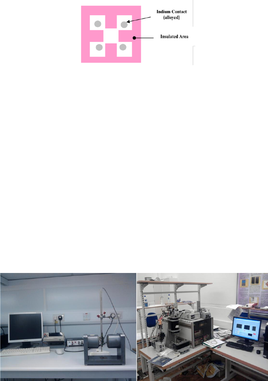
CHAPTER 3
58
Figure 3.3 Van der Pauw geometry Hall Effect sample
In order to form good Ohmic contacts the test sample should be annealed at the proper
temperature (420 ºC for LT GaAs and 310 ºC for LT InGaAs-InAlAs MQWs) in a
Nitrogen (N
2
) atmosphere. The preparation of Hall Effect samples is described in detail in
Appendix A1.
In this work two customised set-ups were used for the Hall Effect measurements. The first
system, which is shown in Figure 3.4 (a), includes a Hall Probe Test Unit and a Fluke 45
Dual Display Multimeter. This multimeter is able to supply a minimum of 10 μA. This set
up is suitable for low resistivity samples. For very high resistivity samples, an alternative
set-up (shown in Figure 3.4 (b)), which contains a Keithley 196 system DMM, Keithley
705 scanner, Keithley 220 Programmable current source and a Keithley 485 Auto ranging
picoameter, can be used. This set-up can supply a minimum current as low a 1 nA. The
second set-up is also able to do the Hall Effect measurements under different temperatures.
Samples were held in an Oxford Instruments liquid nitrogen cryostat model DN1711 and a
LakeShore 330 Autotuning Temperature Controller were used to vary the temperature.
(a) (b)
Figure 3.4 Hall Effect measurements set ups used in this work

CHAPTER 3
59
3.4 Mid-infrared reflectivity measurements
One of the main objectives of this project is to evaluate the optimised photoconductive
materials incorporated with a distributed Bragg reflector (DBR). A DBR is formed by
multiple layers structure of different material with varying refractive index which can
causes a high reflection at a specified wavelength. The periodic layers in DBRs thus act as
a high-quality reflector. The reflectivity measurement is a non-destructive optical
procedure to test the quality of the DBRs at the desired wavelength.
Figure 3.5 Reflectivity measurement system
Figure 3.6 Reflectivity measurement setup
The setup of the mid infrared measurement is shown in Figure 3.6. The source of this mid-
infrared reflectivity measurement is a tungsten halogen broadband source Oceanoptics
LS1
TM
. Two different detectors are used in this work. In the wavelength range of 400 nm
Detector
Broad band
laser source
Coupler
Fibre
head
Sample
Acquisition Data
CHAPTER 3
60
to 1100 nm, a Si CCD array was used. In the wavelength range of 900 nm to 2500 nm an
extended InGaAs detector was used. Depending on the material being tested, each
appropriate detector was used. In order to obtain reliable measurements, a calibration
should be performed before testing the samples. Under dark conditions (source turned off),
the background noise needs to be stored first. The next step is to measure the reflectivity of
a reference sample with the light source on. As the reflectivity of the sample is highly
dependent on the reference sample, a reflectivity of the chosen sample must be set and
stored as the reference before the measurement can be performed.
3.5 Device fabrication
After material characterisations, devices need to be fabricated and tested. The performance
of the device is critically dependent on the geometrical design of the device and their
epitaxial structure.
3.5.1 Mask design
The antenna geometry of the photoconductive materials in this work will be described in
Chapter four and Chapter five. The following sections concentrate only on the mask design
of the ASPAT diodes. The mask was designed using the commercial Advanced Design
Software (ADS) package and patterned as a mask by the CompGraphics Ltd.
In order to work at high frequencies, the mesa area of the diode needs to be small to
decrease the junction capacitance. Such junction capacitance increases the operating
frequency of the device [135]. One of the tasks in this project was to design a mask
including diodes with different dimensions suitable for operation over different frequencies.
In addition, the design should also be compatible with RF measurement, requiring a
‘Ground-Signal-Ground’ (GSG) contact structure.
There were two kinds of mask designs attempted. The first (design 1) was used for
fabricating the GaAs-AlAs ASPAT diodes and relied on a dielectric passivation layer. This
design contains 7 layers in total. The fabrication process steps for design 1 can be seen in
Figure 3.7 (a). The second design (design 2), which includes 5 layers, used the air-bridge
technique. This mask was used for fabricating InGaAs-AlAs ASPAT diodes. The
fabrication process is shown in Figure 3.7 (b). For design 2, step 4 can be neglected as the
pad structure (mask 5) covers the area of the bottom contacts in step 4.

CHAPTER 3
61
(a)
(b)
Figure 3.7 Fabrication process flow for (a) design 1; (b) design 2
Both design 1 and design 2 are suitable for dry and wet etching methods. In this work,
wafer tiles of dimensions 15×15 mm
2
dimensions were diced using standard dicing
procedure of 2”, 3” or 4” wafers. In both designs, the total number of die chips was four
hundred and fifty (450) having eight kinds of mesa areas (100×100 µm
2
, 50×50 µm
2
,
30×30 µm
2
, 20×20 µm
2
, 15×15 µm
2
, 10×10 µm
2
, 6×6 µm
2
and 2×2 µm
2
). For each chip,
the die size is 600 µm×600 µm. The strip width (2a) was designed to be 40 µm while the
spacing between the micro-strip and the ground pad was designed to be 60 µm. The strip
width to ground plane spacing ratio is kept to 0.25, considering the losses in coplanar
waveguides [136]. The ratio equals to 2a/2b as shown in Figure 3.8.
Figure 3.8 Geometry of coplanar waveguide
Step7
Die-bridge
Step6
Passivation
Step1
Top-Contact
Step2
Isolation
Step5
Pad
Step4
Bot-Contact
Step3
Mesa etch
Isolation
Step1
Top-Contact
Step2
Isolation
Step5
Pad
Step4
Bot-Contact
Step3
Mesa etch
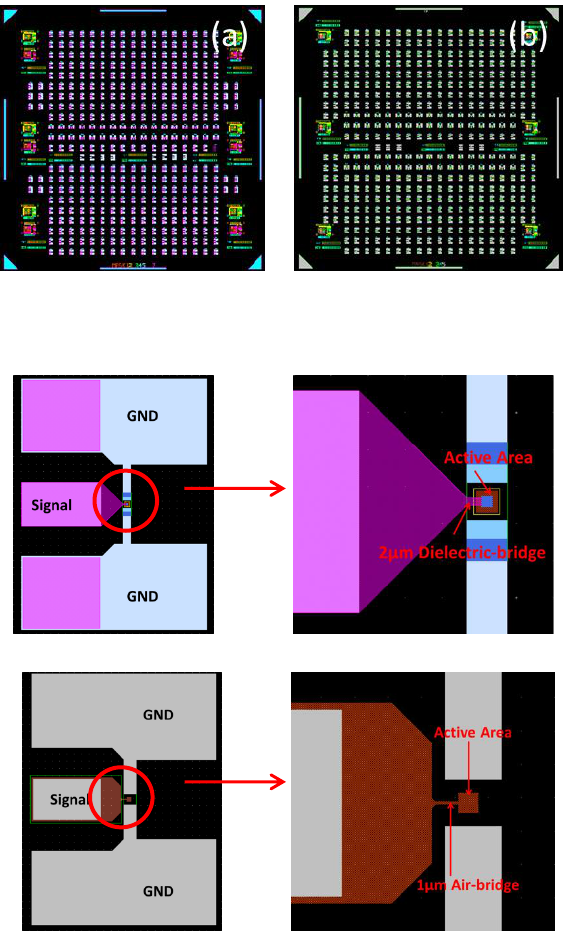
CHAPTER 3
62
To minimise the interaction between diodes as well as to decrease potential current leakage,
the isolation area was designed 5 µm wider from the edge of the contacts. The distance
between top and bottom contacts affect the series resistance of the diode so the tolerance
between contacts was kept at 2 µm. The complete layouts of both designs are shown in
Figure 3.9. The close-up view of a single ASPAT diode with 6 µm×6 µm
mesa area is
shown in Figure 3.10. The dielectric layer is not shown in Figure 3.10 (a) since this layer is
designed as a negative layer for passivation via opening. The working principle of the air-
bridge is described along with the DC properties of the devices in Chapter five.
Figure 3.9 The complete 15×15 mm
2
mask designed using Agilent ADS software (a) dielectric
design (b) air-bridge design
(a)
(b)
Figure 3.10 Close-up view of a single ASPAT diode with 6 µm×6 µm mesa area (dielectric
layer and air-bridge)
CHAPTER 3
63
3.5.2 Fabrication process
The fabrication method used in this work is contact photolithography. Compared with
electron-beam lithography (EBL), photolithography cannot produce features below 500 nm
[137]. However, photolithography is a relatively easier and low-cost way to fabricate
devices. In general, the photolithography method includes tile preparation, spin coating,
exposure and developing [138].
Appendix A2 describes the recipe for the fabrication steps for photoconductive antennas
while Appendix A3 and Appendix A4 show the final recipes for GaAs-AlAs and InGaAs-
AlAs ASPAT diode respectively.
3.5.2.1 Sample Cleaning
For every type of fabrication process, the first step is to clean the sample. Samples were
carefully cleaned using N-Methyl-Pyrrolidone 1165 (NMP) solution, H
2
O, Acetone, and
Isopropanol (IPA). This is important although the fabrication is conducted in the
cleanroom as any contaminants can still affect the performance of the devices. Here, the
contaminants generated by various sources, such as operation crew, facilities in the clean
room and chemical residues. NMP and Acetone are used to remove organic materials while
IPA removes Acetone residues.
The cleaning process in the clean room at room temperature is:
1 Sample is put in NMP solution to eliminate organic residue for 5 mins (in an ultrasonic
bath under power 1)
2 NMP is removed by using de-ionised (DI) water and blown with a nitrogen (N
2
) gun to
dry the sample
3 Acetone is then applied for another 5 mins in an ultrasonic bath
4 IPA is used after Acetone to remove Acetone. This step also takes 5 mins.
5 Due to the rapid evaporation of IPA, the sample needs to be dried using N
2
gun as fast as
possible.
After the sample cleaning steps are completed, the sample is visually inspected under a
microscope to ensure there are no particles on the surface. If an acceptable cleanliness is
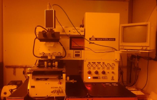
CHAPTER 3
64
not achieved, the cleaning steps need to be repeated. During the entire fabrication process,
visual inspections are taken frequently to ensure adequate cleanliness of the sample surface.
3.5.2.2 Photolithography
In the photolithography technique, the device patterns are transferred onto the surface of
the sample according to the designed mask. This method uses ultra-violet (UV) light with
wavelengths between 200 nm to 450 nm to expose the sample and print the patterns. In this
work, a Karl Suss MA4 mask aligner was used. The source produced a UV light at 365 nm
(i-line) wavelength with intensity at 0.9 mW.
Figure 3.11 Picture of MA4 mask aligner system
The process begins with a spin-coating step. In this step, a thin layer of light-sensitive
material is coated on the surface of the cleaned sample. There are three different types of
light sensitive materials, known as positive, negative and reversible photoresist. The
chemical bonds of the positive photoresist break during exposure to UV light, thus the
remaining positive photoresist keeps the same pattern as the designed structure shown on
the mask. The opening area for this type of photoresist will be slightly larger than the
pattern on the mask due to scattering phenomenon. The negative photoresist when it is
exposed to UV light strengthens its chemical bonds (crosslinking) so that the unexposed
areas are dissolved in a developer while the exposed ones remain. This means that the
remaining negative photoresist shows an opposite pattern to the mask. The opening for the
negative photoresist will be smaller than the designed pattern. In the case of reversible
resist, it can be used as both positive and negative photoresist and the UV light produces a
reversal image.

CHAPTER 3
65
Resist
Mask
Positive resist
Negative resist
Top layer of Semiconductor
Top layer of Semiconductor
Developing and Etching
UV light
Figure 3.12 Pattern differences generated from the use of positive and negative photoresist
[139]
The positive photoresists used throughout in this work are commercially available from
Microposit S1800 series. To be more specific, S1805 and S1813 have thickness of 0.5 µm
and 1.3 µm respectively. Furthermore, negative photoresists with 2.0 µm, 1.0 µm and 0.5
µm thickness supplied by MicroChemicals were also used. In general, positive photoresist
is used for etching steps and negative photoresists are used in single layer lift-off processes
due to their side wall profile.
Figure 3.13 Sample after spin coating stage
The existence of an edge bead (shown in Figure 3.13) will affect the contact between
sample and mask, thus leading to an undesired scattering during exposure. The latter
makes the printed pattern different from the designed one. To avoid the effect of edge
beads, an edge bead remover (EBR) has to be used after spinning off the negative
photoresist for the contact masks.
Edge
Bead
Sample
Photoresist

CHAPTER 3
66
In order to stabilize the photoresist, the samples need to be put on a hot plate or in an oven
after exposure. Different concentrations of developers are used for positive and negative
photoresists. The developer solution for positive photoresist is MF 319 while, MF 326 acts
as a negative photoresist developer solution.
The recipes for use of the photoresists with their corresponding spinner setting and
development times are shown in Table 3-1.
Table 3-1 Photoresists with their corresponding spinner setting and developing times
Photoresist
Thickness
(µm)
Spin
Speed
(r.p.m)
Spin
time
(s)
Exposure
time
(s)
Developer
Development
time
(min)
S1805
0.5
4000
30
22-25
MF319
1
S1813
1.3
4000
30
120
MF319
2
Az 2.0
2
3000
40
5.5
MF326
1
Az 1.0
1
3000
40
8
MF326
1
Az 0.5
0.5
3000
40
12
MF326
1
3.5.2.3 Sample Etching
Etching is one of the main steps in microelectronics manufacturing and it creates well-
defined active area or mesa. Normally, there are two different etching methods: wet and
dry [140]. Wet etching is more common to use as it is usually fast and cost effective. The
etching rate depends on the etchant solution and the operational environment (temperature
and humidity). One disadvantage of wet etching is that it not only etches vertically, but
also laterally (isotropic etching). Basically, the lateral etching is undesirable as it changes
the active area size. However, the opening of air-bridge for InGaAs-AlAs ASPAT diode
relies on this lateral etching. In the case of dry etching, the etching rate is less sensitive to
temperature and more repeatable (anisotropic etching) but relatively expensive. Both
methods are used in this study.
CHAPTER 3
67
(1) Wet etching
The etchant for GaAs-system starts from oxidising the surface and then dissolving the
oxide and hence both Ga and As atoms can be removed. Two groups of etchants were
studied. As the etching rates for the etchants are sensitive to the operating environment
[141], clean room temperature was controlled within 18 °C - 20 °C with the humidity from
47%-61% throughout these studies. Orthophosphoric-based etchants are mixtures of
Orthophosphoric acid, Hydrogen Peroxide and DI Water (H
3
PO
4
: H
2
O
2
: H
2
O). For each
solution, there were at least forty runs (including calibration samples and real samples) for
GaAs and InGaAs. The average etching rates for GaAs and InGaAs using
Orthophosphoric-based etchants with ratios of H
3
PO
4
: H
2
O
2
: H
2
O=2:1:2, H
3
PO
4
: H
2
O
2
:
H
2
O=1:1:38 and H
3
PO
4
: H
2
O
2
: H
2
O=3:1:50 are shown in Figure 3.14.
By using H
3
PO
4
: H
2
O
2
: H
2
O=2:1:2, the average etching rates for GaAs and InGaAs are
48nm/sec and 39nm/sec respectively. Throughout the fabrications in this work, the highest
etching rates using H
3
PO
4
: H
2
O
2
: H
2
O=2:1:2 for GaAs and InGaAs are 52 nm/sec and
45nm/sec while the lowest rates were 43 nm/sec and 35 nm/sec respectively. As the
etching rates using H
3
PO
4
: H
2
O
2
: H
2
O=2:1:2 are faster, during the process, the etching
time should be well controlled, down to seconds. In the case of GaAs, using H
3
PO
4
: H
2
O
2
:
H
2
O=1:1:38 and H
3
PO
4
: H
2
O
2
: H
2
O=3:1:50, the highest etching rates variation were 0.05
nm/sec for both etchants. For InGaAs, only H
3
PO
4
: H
2
O
2
: H
2
O=3:1:50 were used, and the
variation was about 0.1 nm/sec. Since the etch rate is small in comparison to other
concentrations, there is no need to control the etching time to the one second precision.
Thus, the etching time for H
2
O
2
: H
2
O=1:1:38 and H
3
PO
4
: H
2
O
2
: H
2
O=3:1:50 were
normally controlled to within one minute or half a minute.

CHAPTER 3
68
2:1:2
1:1:38
3:1:50
0 10 20 30 40 50
~ 1.5±0.05 nm/second
~ 1±0.05 nm/second
43~52 nm/second
(a): GaAs
Etching Rate (nm/second)
H
3
PO
4
: H
2
O
2
: H
2
O
2:1:2
3:1:50
0 10 20 30 40
~ 1.3±0.1 nm/second
~39 nm/second
(b): InGaAs
Etching Rate (nm/second)
H
3
PO
4
: H
2
O
2
: H
2
O
Figure 3.14 Average etching rates for (a) GaAs and (b) InGaAs using Orthophosphoric-based
etchant at different ratios
By using the Orthophosphoric-based etchants, the absolute vertical cross-sectional
structure cannot be achieved. In the case of the InGaAs material system, the cross-sectional
views of the device are depicted in Figure 3.15.

CHAPTER 3
69
Metal
Metal
AlAs
AlAs
InGaAs (n++)
InGaAs n++
InP(SI)
InGaAs (n++)
Metal
Metal
AlAs
AlAs
InGaAs(++)
InGaAs n++
InP(SI)
InGaAs (n++)
(a) (b)
Figure 3.15 Cross sectional view of InGaAs device (a) ideal etch (b) practical wet etch
The Ammonium Hydroxide: Hydrogen Peroxide: DI Water (NH
4
OH: H
2
O
2
: H
2
O) was
reported as a highly anisotropic wet chemical etching for 2° mis-oriented GaAs substrate
[142]. This etchant can be useful to vertically etch GaAs samples. The etching rates for
GaAs with Ammonium Hydroxide- based etchants with different ratios are shown in
Figure 3.16.
1:1:8
1:1:18
1:1:40
0 5 10 15 20 25
~ 4.7 nm/second
~ 15.2 nm/second
~26 nm/second
GaAs
Etching Rate (nm/second)
NH
4
OH : H
2
O
2
: H
2
O
Figure 3.16 Average etching rates for GaAs using Ammonium Hydroxide-based etchants
The etching rates for Ammonium Hydroxide-based etchant were tested with three different
ratios: NH
4
OH: H
2
O
2
: H
2
O=1:1:8, NH
4
OH: H
2
O
2
: H
2
O=1:1:18 and NH
4
OH: H
2
O
2
:
H
2
O=1:1:40. The deviation between each run can be up to 3 nm/sec, 0.7 nm/sec and 0.5
CHAPTER 3
70
nm/sec respectively. Amongst all three etchants, NH
4
OH: H
2
O
2
: H
2
O=1:1:40 showed the
best stability, thus this etchant was used for wet etching the GaAs samples.
As can be seen in Figure 3.14 and Figure 3.16, the etching rates did fluctuate. This is due
to the variation of temperature and humidity of the clean room during processing. Thus,
calibration before each is extremely important, especially if the samples need careful
control of etching depths.
(2) Dry etching
Compared to wet etching, dry etching can provide higher resolution anisotropic etching
[143]. There are several dry etching techniques commonly used. The first type is ion
milling [144]. The energetic noble gas ions, such as Argon (Ar +), bombard the sample
surface and erosion occurs by physically knocking atoms off the surface. This method
provides highly anisotropic etching, but significant displacement damage which can extend
to hundreds of nanometres into the material. The second method uses plasma which
contains ions, free radicals and by-products. The material erosion occurs when free radicals
and by-products decrease the activation energy (in chemical reaction) [145]. The method
used in this work was the reactive ion etching (RIE), and the schematic of a RIE system is
shown in Figure 3.17. In the reactive gas, an applied radio frequency (13.56 MHz) between
two parallel electrodes generates the plasma. The electric field across the area between the
plasma and electrodes (plasma sheath) leads to the accelerations of ions at the edge of the
plasma across the plasma sheath. The sample which is placed on the cathode is targeted by
the ion bombardment, neutral gas atoms and molecules from the plasma[146]. The class of
gas mixture used in this work is based on methane (CH
4
) and hydrogen (H
2
). This mixture
can etch both gallium- and indium- based semiconductor smoothly and is highly
anisotropic. The etch products for this mixture can be AsH
3
(or PH
3
) and (CH
3
)
n
Ga (most
probably methyl adduct) for group V and III species respectively [147].
In this work, samples used the deposited metal (top contact) as the mask while S1805 was
used to protect the TLM pattern (See Section 3.6). Material such as C
n
H
m
X can remain on
the surface of the sample which obstructs the etching reaction [148]. Thus, in the dry
etching process, the system settings need to be well controlled to reduce the polymer
residues. The sample was etched at a forward biased power of 150 W with a gas flow for
CH
4
of 10 sccm and H
2
of 80 sccm providing a pressure of 42 mTorr. Under these

CHAPTER 3
71
conditions, the etching rate of GaAs and InGaAs were 15±5 nm/min and 21±3 nm/min
respectively. After each run of the semiconductor etching, a polymer removal step needs to
be followed. This is done by using a forward power of 100 W oxygen (O
2
) flow of 30 sccm
under 100 mTorr.
Figure 3.17 Schematic of RIE system
3.5.2.4 Post growth annealing
The post growth annealing is an essential step specifically for low temperature grown
photoconductive materials. It was proved to improve the crystallinity and the structural
integrity of the epilayers [149]. In addition, the strain in the lattice caused by the excess
arsenic relaxes. Gregory et al have reported the effects of post growth annealing on LT
GaAs material [90]. Sometimes, due to the characteristics and properties of the material,
annealing cannot be done during the growth process and samples need to be annealed ex-
situ. A Rapid thermal annealer (RTA) allows the formation of precipitates from the arsenic
excess incorporated as point defects [21]. Post growth annealing in this work was
performed in all the samples using a Process Products Corporation Rapid Thermal Module.
A picture of the RTA is shown in Figure 3.18.
Cooling water
Cathode
Plasma
Chamber
Substrate
Anode
Plasma
Sheath
Reactive gasses & Nitrogen
R
F

CHAPTER 3
72
Figure 3.18 Rapid Thermal Annealer used in this work
The annealing process can change the properties of the material. The characterization of
samples under different annealing temperature and time were described by our group
before [150]. The consequence of annealing the samples was a significant decrease in the
residual carrier density. The group showed previously that the characteristics are improved
significantly by annealing the material in the range of 500-600 °C for 10-15 minutes. For
LT GaAs and LT InGaAs-InAlAs MQW samples, the optimum RTA temperatures used in
the fabrication process were set to 580 °C and 600 °C respectively. During the annealing
process, samples were covered by high purity SI GaAs substrates to prevent arsenic loss
from the sample surface and annealed in an N
2
environment for 10 min.
3.5.2.5 Metallisation
In order to make working devices, the fabricated semiconductor device should be able to
be connected to components in the outside world. This means that the deposition of a
conductive material (metal) on the surface of the device is necessary. There are several
methods used for metal deposition such as Filament Evaporation, Electron-Beam
Evaporation and Sputtering [151]. The technique used in this work was based on the
filament evaporation technique. The filament current of a boat is increased until the metal
starts to melt and evaporate. Two evaporators were used in this work. For the
photoconductive antennas, a BioRad evaporator was used. The picture of this equipment is
shown in Figure 3.19 (a). Before metal deposition, the patterned sample was de-oxidized in
a HCL: H
2
O=1:1 solution. For the photoconductive antennas, a 1.5 cm Titanium (Ti) and a
5 cm Gold (Au) were loaded in separate boats in the evaporator. This resulted in final

CHAPTER 3
73
metal contacts with thickness of 50 nm for Ti and 100 nm for Au. The process conditions
require a low-pressure environment (10
-6
mbar) to minimise contaminations and reduce
scattering. In the case of the ASPAT diodes, this process is performed using an Edwards
Auto 306 (shown in Figure 3.19 (b)) which has a lower base pressure of 10
-7
mbar. For
ASPAT diodes, the same metals are evaporated with contact thickness of 55 nm for Ti and
250 nm (minimum) for Au.
(a) (b)
Figure 3.19 Evaporator set-ups (a) Bio Rad and (b) Edwards Auto 306
3.5.2.6 Lift-off
After metallisation, a uniform metallic film is evaporated on the material surface. The
purpose of lift-off is to remove any undesired metal. This is based on the elimination of the
deposited photoresist in the previous spin-coating step. Figure 3.20 shows the lift-off
process with a negative photoresist undercut profile.
Figure 3.20 Lift-off process with the negative photoresist undercut profile

CHAPTER 3
74
3.5.2.7 Annealing
Annealing is a critical step for all devices fabricated in this work. For contacts, annealing
forms an Ohmic contact with a smaller contact resistance compared with the un-annealed
sample. The annealing temperature for the photoconductive antennas was 250 ºC for 1 min
using an alloying jig. For the ASPAT diodes, the samples were kept into a furnace for 2
mins at 420 ºC (GaAs sample) or 280 ºC (InGaAs sample). Pictures of the annealing
equipment are shown in Figure 3.21.
(a) (b)
Figure 3.21 Annealing equipment (a) alloying jig and (b) furnace
3.6 Current-Voltage testing
The current-voltage testing is the step following the fabrication process. The electronic
characteristics of devices can be obtained in this step. Moreover, the I-V testing is a useful
tool to check the quality of the fabrication process. An Agilent Technologies B1500A
semiconductor devices analyser was used for the I-V measurement at room temperature in
this work. In addition, it is also common to perform the measurements at different
temperatures. The temperature variation measurements were performed using a Lakeshore
Cryogenic probe station. As liquid Nitrogen was used to cool down the system, the lowest
temperature possible was 77 K. In order to protect the sample holder, the highest
temperature was limited to 400 K. In that set-up the temperature could be maintained
within ±0.1 K around the nominal value during data acquisition. To avoid the influence
from light, all measurements were performed under dark conditions. The IC-CAP software
program with predefined voltage and current compliances were used to acquire and analyse
the data.

CHAPTER 3
75
(a) (b)
Figure 3.22 Pictures of (a) B1500A semiconductor device analyser and (b) Lakeshore
Cryogenic probe station used in this study
The metal-semiconductor contacts play a vital role for the semiconductor device
characteristics hence the contact should be evaluated. In this project, in order to assess the
metal-semiconductor contact, the transmission line model (TLM) technique was used [152].
d
n
Metal contact
Semiconductor
Substrate
d
3
d
2
d
1
V
A
Figure 3.23 Four-Point probes TLM measurements set up
The side-view for a typical Four-point probes TLM structure is shown in Figure 3.23. It
consists of a series of metal contacts with different separations d
n
(n=1,2,3,4,5) in between.
The separations of TLM testing pattern used in this work were from 5 µm up to 45 µm
with a 5 µm increase step. These contacts are placed on a thin conducting layer (heavily
doped material). This structure allows current to flow in the direction defined by the
pattern.
The top view of this structure is illustrated in Figure 3.24. All the metal pads are defined
with the same size with a length of l and width w. L
T
is the transfer length (effective length)
where most of the current flows into the semiconductor.

CHAPTER 3
76
Top View
L
T
d
1
L
T
d
2
w
l
Figure 3.24 Schematic drawing for top-view of TLM structure
From the TLM measurements, a linear plot of the resistance versus distance can be
obtained (as shown in Figure 3.25).
Figure 3.25 Plot of resistance versus spreading distance in TLM structure
Two key values can be extracted from this plot. The first one is the contact resistance R
c
which can be evaluated from the slope of the plot. Assuming the contact resistances R
c
are
the same, thus the total resistance R
total
between the first and second contact is given by:
where R
sh
is the sheet resistance (in Ω/sq).
The second key value is the transfer length L
T
. When R
total
=0, the interception of the
measured line with the separation-axis gives a value of 2|L
T
|.

CHAPTER 3
77
Once the values of contact resistance R
c
and transfer length L
T
are extracted, the series
resistance R
s
of the fabricated diodes can be calculated. In the case of the RTD diode, R
s
includes the contact resistance, resistance due to the epi-layers R
epi
and the spreading
resistance from the bottom contact layer [153]. The series resistance for the ASPAT diode
can be calculated by the same method.
Figure 3.26 Cross section of an ASPAT showing the epi-layers and contacts
Based on R
c
and L
T
obtained from TLM measurement, the specific contact resistance can
be expressed as [154]:
where l
c
is the length of the contact pad.
The resistance of the epi-layers R
epi
can be given by the following equation:
where and l
epi
represent materials resistivity and the thickness of specific epilayers while
A refers to the active mesa area of the diode.
The spreading resistance R
spr
can be approximated as [39]:

CHAPTER 3
78
where is the conductivity of the bottom ohmic layer (Ohmic 2) and d
ohmic2
is the
thickness of Ohmic 2. In addition, a
mesa
is half of the length of the device length, a refers to
the length indicated in Figure 3.26.
Hence, the series resistance of the ASPAT diode is calculated by dividing the specific
contact resistance to the diode active mesa size and adding the epi-layer resistance R
epi
, and
spreading resistance R
spr
:
The series resistance decreases with increasing device mesa area. Lowering the ASPAT
series resistance is a must for operation at THz frequencies.
3.7 Radio frequency (RF) measurements
RF measurement is an on-wafer measurements technique used to perform microwave
characterisation of devices. In this work, an Anritsu 37369A vector network analyser
(VNA) was used to acquire the scattering parameters (S-parameters) from 40 MHz to 40
GHz. The VNA is the key instrument to accurately measure the scattering parameters of
devices in the microwave and millimetre wave ranges [155]. The fabricated GSG-designed
ASPAT diodes were tested for each emitter dimension at room temperature using the
equipment shown in Figure 3.27. The results from this experiment would provide an
optimum design in terms of yield versus performance, providing a suitable reference for
future work.
Figure 3.27 Photo of VNA system set up
CHAPTER 4
79
CHAPTER 4: LOW TEMPERATURE GROWN
PHOTOCONDUCTIVE MATERIALS INCORPORATING
DISTRIBUTED BRAGG REFLECTORS
4.1 Introduction
Even though the LT GaAs and LT InGaAs-InAlAs MQWs already showed good
performances in TDS applications, the demand for high output THz power still remains for
real time, fast acquisition data. Since the number of photo-carriers generated by
illumination is the key factor in determining the efficiency of THz photoconductive
devices, finding a way to generate more photo-carriers is essential to improve the
performance of this type of THz devices. The photo-carrier generation is related to the
strength of the electric field and the absorption coefficient of the photoconductive material.
In the first case, the decay of the electric field strength can be prevented by vertically
biasing the device [22]. In the second case, distributed Bragg reflector (DBR) layers can be
incorporated during the growth process [156]. This work concentrates on the second case.
Taylor and Brown have reported a significant improvement of the photoconductive
switches performances by using a resonant-optical-cavity at 300 GHz [157]. The main idea
for this chapter is to investigate photoconductive antenna performances incorporating with
DBR layers.
This chapter includes a description of the epitaxial layers and doping profiles of the low
temperature grown photoconductive materials incorporating DBRs. An extensive material
characterisation and photoconductor antennas fabrication processes are presented. The
summarised results from the measurements are then compared with conventional
photoconductors. In addition, the fabricated transmitters and detectors are evaluated in a
TDS system under pulsed operation. The characteristics of this optimised THz devices
with DBR under the active layers revealed enhanced THz output power leading to further
improvements in the performance of these already efficient devices.
The next part of this chapter introduces details of a home built 1.55 µm THz spectrometer
with its key elements (emitter and detector) fabricated using the LT InGaAs-InAlAs

CHAPTER 4
80
MQWs photoconductive material. A series of measurements using the full 1.55 µm THz
spectrometer are also presented in this chapter.
4.2 LT GaAs DBRs structure
The THz photoconductive devices are based on laser-driven excitation. The relationship
between the energy of a photon and the laser wavelength of the light (λ) is given by:
where h is Planck’s constant and c is the speed of light. The Equation 4.1 can be rewritten
as:
Currently, LT GaAs is the most promising photoconductive material as it presents a high
resistivity, high electron mobility and ultrafast carrier lifetimes [90]. To date, this type of
photoconductor is widely used in various optoelectronic THz applications. However, as the
bandgap of this material is 1.42 eV at room temperature, the driving laser of the THz
system should be operated at wavelengths around 800 nm. Such lasers can be femtosecond
pulse Ti: Sapphire lasers and generate broadband pulsed THz radiation [73, 74].
However, even using LT GaAs as the transmitter and receiver in the THz system, the
output power still hasn’t reached desirable levels. Thus, an optimised LT GaAs
incorporating DBRs was developed.
In this section, two samples were evaluated. The first sample is a LT GaAs labelled as
XMBE305, which was grown on a SI-GaAs substrate, and consists of a 240 nm GaAs
buffer layer followed by a 50 nm AlAs layer and a 1 µm thickness low temperature grown
GaAs layer. The optimised LT GaAs labelled as XMBE316 wafer has the same thickness
of low temperature grown GaAs layer, but it has in addition 8 pairs of GaAs-AlAs DBR
layers (centered around 800nm) between the low temperature grown GaAs and the 100 nm
GaAs buffer layer. The total thickness of the DBR is 1.02 µm. Figure 4.1 illustrates the
physical structures along with the layer thicknesses XMBE 305 and XMBE 316.

CHAPTER 4
81
(a)
LT GaAs
AlAs
GaAs
GaAs (SI)
1000 nm
50 nm
240 nm
(b)
LT GaAs
GaAs
AlAs
GaAs
1000 nm
62.6 nm
66 nm
GaAs (SI)
100 nm
8 times
Figure 4.1 Physical structures along with the layer thicknesses of (a) XMBE 305 and (b)
XMBE 316 (Both structures were designed to operate at 800 nm wavelength)
Both the GaAs and AlAs layers are λ/4 thick at 800 nm (with GaAs thickness=
800/4×3.2=62.6 nm, refractive index is 3.2 and AlAs thickness=800/4×3.02=66 nm,
refractive index is 3.02).
Note that the simulation module used in this work is the Reflection Calculator provided by
FILMETRICS based on the complex-matrix of Fresnel Equation. Up to 20 films can by
simulated in this system. Figure 4.2 shows the reflectance as a function of wavelength for
the GaAs-AlAs DBRs. From this figure, the reflectance bandwidth of the GaAs-AlAs
DBRs can be obtained.
650 700 750 800 850 900 950 1000
0.1
0.2
0.3
0.4
0.5
0.6
0.7
0.8
0.9
1.0
Reflectance
Wavelength (nm)
10 pairs
8 pairs
6 pairs
4 pairs
Figure 4.2 Reflectance as a function of wavelength (GaAs-AlAs DBRs)
From Figure 4.2, it can be seen that when applying more GaAs-AlAs pairs, the bandwidths
of the DBR layers decreases while the reflectance increases. The peak reflectance is

CHAPTER 4
82
achieved at 880 nm. The full width at half maximum (FWHM)/reflectance bandwidths for
this type of DBRs decreased from 210 nm to 128 nm when using 4 pairs or 10 pairs of
GaAs-AlAs. The reflectance at 800 nm (designed wavelength) and 880 nm (peak
reflectance wavelength) are listed in Table 4-1. The FWHM of the DBRs are also listed in
this table.
Table 4-1 The reflectance of GaAs-AlAs DBRs
Pairs of GaAs-AlAs
Reflectance at 800 nm
Peak Reflectance
(obtained at 880 nm)
FWHM
(nm)
2
0.54
0.58
4
0.64
0.68
180
6
0.68
0.86
150
8
0.70
0.92
134
10
0.70
0.95
124
As can be seen in Table 4-1, with an increase in the number of GaAs-AlAs DBR pairs, the
reflectance gets higher. The reflectance at 800 nm increased significantly when the GaAs-
AlAs increased from 2 to 4 pairs. Even through, the reflectance of the GaAs-AlAs DBRs
haven’t reach the high reflectance range ( higher than 97%), eight pairs of GaAs-AlAs still
results in a reflectance of 0.7 at 800 nm and 0.92 at peak reflectance wavelength. This
changes only slightly with further increase of DBR pairs up to 10. Therefore larger number
of GaAs-AlAs pairs can result in a higher reflectance. The design of the DBRs in
XMBE316 only repeats the GaAs and AlAs layers (with thicknesses of 62.6 nm and 66 nm
respectively) 8 times but was able to achieve a high enough reflectance at 800 nm. As the
main purpose of this optimisation is not the design of a very high reflectivity DBR, the
resulting reflectance is high enough. The advantage of reducing the periodicity to 8 also
reduces the growth time for the fully optimised LT GaAs materials with DBRs.
As can be seen in Figure 4.2, the 800 nm is located at the rising edge of the DBRs. In order
to further optimise the DBR design, the thickness of GaAs can be reduced. This can not
only help to increase the reflection at 800 nm, but also help to further decrease the growth
time. The simulated reflections of the DBRs with 8 pairs GaAs-AlAs material system
(58nm of GaAs and 66nm of AlAs for each pair) are shown in Figure 4.3.

CHAPTER 4
83
In the case of this optimised design, the peak reflectance is only 0.86 at 815 nm, which is
not as high as the original design. However, the reflection at 800 nm shows a much higher
reflection of 0.85 compare with the original design and is now located much closer to the
peak reflection wavelength (815 nm). In this case, the optimised GaAs-AlAs material
system showed a FWHM of 137 nm. This center wavelength shifting is due to the fact that
the simulation module takes into account the material refractive index changes at different
wavelengths.
650 700 750 800 850 900 950 1000
0.1
0.2
0.3
0.4
0.5
0.6
0.7
0.8
0.9
1.0
Reflectance
Wavelength (nm)
original
optimised
Figure 4.3 Comparison of the reflection for 8 pairs of GaAs-AlAs DBRs with theoretical
thicknesses and the optimised thicknesses
4.2.1 Mid-Infrared reflectivity measurements
The reason for using DBR is to enhance the absorption coefficient of the photoconductive
devices. The DBR layers incorporated with photoconductors had been proved to improve
the antenna performance for both emitters and detectors [156, 158]. In the case of
XMBE305 material system, only a part of the incident power is absorbed by the active
layers (low temperature grown layers). However, with the help of the DBR layers, most of
the not-absorbed radiation is reflected back towards the active layers. To show evidence of
this reflectance, the reflectivity at the working frequency of 800 nm for XMBE316 was
tested using Mid-Infrared reflectivity measurements. In this measurement, an Ocean Optics
LS1 tungsten halogen light source and an Ocean Optics S200 CCD detector were used. As
mentioned in Chapter three, the reference used in the reflectivity measurements is vital.
The reference used here was the as grown XMBE305 and its reflectivity was set to as
100% by the software. Under this condition and by etching the test sample (XMBE316) at

CHAPTER 4
84
different depths, the effect of the DBR layers can be evaluated. For this reason, two
XMBE316 samples were prepared using a wet etching method. The first one etched
marginally above the DBR layers (960 nm) while the second one etched into the DBR
layers (1020 nm). Figure 4.4 shows the normalized reflectivity of these two samples.
700 720 740 760 780 800 820
0
50
100
150
200
250
300
As grown sample: Etched 960nm
As grown sample: Etched 1020nm
As grown sample: As reference
Normalised
Reflectivity to as grown sample
(%)
Wavelength
Figure 4.4 Normalised reflectivity of XMBE316 with different etching depths
The dotted red line in Figure 4.4 shows the contribution of both active and DBR layers.
Compared with the reference sample (blue dashed line), this sample had a majority of the
active layer removed. Thus, the normalized reflectivity for this sample shows a much
higher value than the reference at specific wavelengths due to the thicker active layer
absorbing more incident light in the reference. The dotted line gives further evidence of
this explanation and also shows that the design of the DBR layers can reflect radiation at a
specific wavelength as the low temperature grown material had been removed and all DBR
layers were remained. From the reflection trend shown in Figure 4.4, the 800 nm point is
located at the rising edge which is in good agreements with the data obtained from the
reflection calculator.
4.2.2 Hall Effect
Hall Effect measurements were performed to check whether the DBR layers affect the
mobility or not. Samples XMBE305 and XMBE316 were prepared and tested under the
same conditions. Both Hall Effect samples were annealed at 600 ºC for 10 mins and
etched till the substrate using a standard ‘cloverleaf’ pattern. For each sample, four pieces

CHAPTER 4
85
of Indium alloys were used as Ohmic contacts at the corners of the sample. Figure 4.5
shows an example of the cloverleaf patterned Hall Effect sample.
Figure 4.5 Photo of Cloverleaf Van der Pauw geometry Hall Effect sample
The results from Hall Effect are shown in Table 4-2 for both XMBE305 and XMBE316
samples.
Table 4-2 Hall Effect measurements of LT GaAs samples
GaAs samples
Annealing Temperature: 600˚C
Sample ID
Mobility
(cm
2
/Vs)
Concentration
(cm
-3
)
Sheet resistance (Ω/sq)
XMBE305
2401
2.79×10
10
9.33×10
8
XMBE316
2190
2.95×10
10
9.67×10
8
At room temperature under dark condition, the conventional LT GaAs sample (XMBE305)
exhibited a mobility of 2401 cm
2
/Vs, carrier concentration of 2.79×10
10
cm
-3
, and a
calculated sheet resistance of 9.33×10
8
Ω/sq. In the case of the LT GaAs incorporating the
DBR (XMBE316) sample, the mobility was measured to be 2190 cm
2
/Vs, with a carrier
concentration of 2.95×10
10
cm
-2
, thus the sheet resistance was then calculated to be 9.67
×10
8
Ω/sq. Both samples exhibited a similar mobility and carrier concentration and thus
similar sheet resistance. The latter indicates that DBR layers do not affect the electronic
properties of the LT GaAs samples. Note that the exceptionally high values of sheet
resistances imply that it is mainly the substrates that are being measured.
4.2.3 Antenna Characterisations
After the optical and electronic characterisations, antennas with different geometries were
fabricated on the samples (shows in Figure 4.6). The aperture antennas were designed to be

CHAPTER 4
86
3.5 mm height, 500 µm width with 400 µm gap. While the dipole antennas have the same
height and width as the aperture antennas but with a 5 µm gap between the arms with a
length of 20 µm.
400µm
3.5mm
Apertures
Bias pad
500µm
500µm
5µm
3.5mm
Dipole
Bias pad
Bias pad
(a) (b)
Figure 4.6 Antenna geometries (a) Aperture and (b) Dipole
The aperture structures were used as emitters while the dipole antennas were used as
detectors in the THz TDS system. The evaluation was performed at room temperature
under pulsed excitation. The detailed TDS system description under pulsed operations was
explained in Chapter two. In the 800nm setup system, a Mai Tai pulse laser from Spectra
Physics was used. The pump beam was focused onto the emitter surface and the probe
beam was focused onto the detector after delay. At the back side of emitter and detector, a
high resistivity hyper-hemispherical Si lenses were attached to collimate and focus the THz
radiation. The system used in this section was operated at 800 nm, with an optical pulse
duration of 100 fs and pulse repetition rate of 80 MHz. The power of the pump beam and
probe beam were 25 mW and 10 mW respectively.
To investigate the improvement by using the LT GaAs photoconductive antenna with
DBRs, both XMBE305 and XMBE316 were tested and evaluated under the same
conditions. There were two measurements performed. In the first one, the aperture used as
emitter and the dipole as detector were both fabricated on sample XMBE305. In the second
measurement, the detector was kept the same but as emitter an aperture antenna fabricated
on sample XMBE316 was used. Both emitters were biased at 50 V. Figure 4.7 illustrates
the emitted THz pulses and their normalized Fourier power spectrum for both setups.

CHAPTER 4
87
Figure 4.7 (a) THz pulses and (b) normalized Fourier transform power spectrum emitted
from large aperture antenna fabricated on the XMBE316 (LT GaAs with DBR) and detected
by a dipole antenna fabricated on the XMBE305 (LT GaAs)
Figure 4.7 depicts the THz pulse emitted from the optimised LT GaAs photoconductive
antenna and the calculated Fourier power spectrum. The FWHM in the THz pulse figure
gives an indication of the material carrier lifetime and the field amplitude indicates the
strength of the THz signal.
The THz peak signal for XMBE316 was 11.5 nA with FWHM of 0.533 ps. The 20 dB
bandwidth for this measurement indicates a spectral extent around 1.45 THz. In addition,
the power to noise ratio is more than 60 dB with frequency extending up to 3.5 THz. In
comparison to the conventional LT GaAs system (using XMBE305 as emitter), the
optimized system shows a 0.02 ps smaller FWHM. This means the XMBE316 antenna has
a slightly faster photoconductive switch speed than that of sample XMBE305.
CHAPTER 4
88
Furthermore, under 50 V bias, the photocurrent measured at the XMBE316 large aperture
antenna side was 1.8 µA which was more than double of the photocurrent generated by
XMBE305 with the same antenna geometry design under the same bias voltage. The
relative THz power can be in arbitrary units by taking into account the measured current
and the incident THz electric field. Therefore, the relative magnitudes of the THz power of
XMBE305 and XMBE316 are 2050 and 6900 respectively. Considering the photocurrent
and the probe beam power, the responsivities of XMBE305 and XMBE316 are 0.57
nA/mW and 1.15 nA/mW. In addition, the system using sample XMBE316 also shows a
0.12 THz wider 20 dB bandwidth.
Thus, the conclusion after comparing the two systems is that DBRs under LT GaAs active
layers slightly shorten the switching speed and enhance the THz peak signal by more than
twice as well as increasing the transmitter photocurrent.
4.3 LT In
0.53
Ga
0.47
As-In
0.52
Al
0.48
As MQWs DBRs structure
LT GaAs and its optimised material show properties that fulfil all the requirements for an
efficient THz TDS. However, femtosecond laser used in 800 nm system is bulky and costly
thus limiting its widespread usage. In order to build a cheaper and portable TDS system,
alternative materials which are compatible with lasers operating at longer wavelengths are
required. These materials should also have similar properties as LT GaAs but a smaller
bandgap. The most desired lasers operate at the telecommunication wavelength of 1.55
µm. Therefore, a cost effective material system candidate can be the LT InGaAs-InAlAs
MQWs. In this work, the materials used to be excited at the 1.55 µm wavelength were
grown on a semi-insulating iron-doped InP substrate (SI InP) with a Be doped LT InGaAs-
InAlAs MQWs epitaxial layers. This design was inspired from an initial material system
reported by Chen et al [105]. Two LT InGaAs-InAlAs MQWs samples were evaluated.
Both samples were grown in the V100HU MBE system in the University of Manchester.
The first one, XMBE290, was grown on a SI-InP substrate following a normal temperature
grown 100 nm InAlAs buffer layer. The active layers were all grown at low temperature
and consisted of a 50 periods of 12 nm In
0.53
Ga
0.47
As and 9 nm In
0.52
Al
0.48
As super lattice
structure and an In
0.53
Ga
0.47
As cap layer. Be atoms were uniformly doped throughout all
active layers with a doping concentration of 2×10
18
cm
-3
. The second one, XMBE329, was
similar to XMBE290, having a slightly thicker barrier (from 9 to 12 nm) which however

CHAPTER 4
89
does have any effect on the designed wavelength of 1550 nm. Additionally, 8 pairs of
In
0.53
Ga
0.47
As-In
0.52
Al
0.48
As DBRs were grown in between the InP and active layers at
normal temperature for XMBE329. Each pair contained a 103.3 nm InGaAs and 103.3 nm
InAlAs. Both structures of XMBE290 and XMBE329 are shown in Figure 4.8.
(a)
LT-InGaAs(Be)
120 Å
90 Å
120 Å
900 Å
LT-InAlAs(Be)
LT-InGaAs(Be)
LT-InAlAs
InP(Fe)
50 times
(b)
LT-InGaAs(Be)
120 Å
120 Å
1033 Å
1033 Å
LT-InAlAs(Be)
InGaAs
InAlAs
InP(Fe)
50 times
8 times
Figure 4.8 Physical structures along with the layer thicknesses of (a) XMBE 290 and (b)
XMBE 329 (Both structures were designed to operate at 1550 nm)
The design for the InGaAs-InAlAs DBRs was similar to that of the GaAs-AlAs DBRs.
Both the InGaAs and InAlAs layers are λ/4 thick at 1550 nm (with InGaAs thickness=
1550/4×3.8=102 nm, refractive index is 3.8 and AlAs thickness=1550/4×3.6=107.6 nm,
refractive index is 3.6). In order to simplify the growth process and taking into account the
refractive index at the main wavelength, both InGaAs and InAlAs were designed to have a
thickness of 103.3 nm.
Figure 4.9 shows the reflectance as a function of wavelength for InGaAs-InAlAs DBRs.
From this figure, the reflectance bandwidth of the InGaAs-InAlAs DBRs can be obtained.
1100 1200 1300 1400 1500 1600 1700 1800 1900
0.2
0.3
0.4
0.5
0.6
0.7
Reflectance
Wavelength (nm)
10 Pairs
8 Pairs
6 Pairs
4 Pairs
Figure 4.9 Reflectance as a function of wavelength (GaAs-AlAs DBRs)

CHAPTER 4
90
From Figure 4.9, it can be seen that when using more InGaAs-InAlAs pairs, the
bandwidths of the DBR layers decreases while the reflectance increases. The peak
reflectance is achieved at 1520 nm. Due to the light absorption property of InGaAs
material near 1550 nm, the peak reflectance did not reach a high reflectance range
(reflectance higher than 0.9) even for 10 pairs of InGaAs-InAlAs DBR layers. However,
the InGaAs-InAlAs still show a good enough DBR quality to fulfill the demand of this
project. The bandwidths for this type of DBRs decrease from 473 nm to 159 nm when
using 4 pairs or 10 pairs of InGaAs-InAlAs. The reflectance at 1550 nm and 1520 nm are
listed in Table 4-3. The FWHM of the DBRs are also listed in the table.
Table 4-3 The reflectance of GaAs-AlAs DBRs
Pairs of GaAs-AlAs
Reflectance at 1550 nm
Peak Reflectance
(obtained at 1520 nm)
FWHM
(nm)
4
0.44
0.44
473
6
0.51
0.52
274
8
0.57
0.59
197
10
0.62
0.65
159
As can be seen in Table 4-3, more InGaAs-InAlAs DBR pairs lead to higher reflectance.
The reflectance at 1550 nm increased significantly when using 4 to 6 pairs InGaAs-InAlAs
layers. In the case of the InGaAs-InAlAs material system, 1550 nm is close enough to the
center wavelength obtained (1520 nm) and does not show much differences in terms of the
reflectance. In order to shorten the growth time, the design of the DBRs in sample
XMBE329 uses 8 pairs of InGaAs and InAlAs with a common thickness of 103.3 nm. The
reflection value also indicates that this design is able to result in a high enough reflectance
at 1550 nm.
4.3.1 Mid-Infrared reflectivity measurement
To study the optical effect of the DBRs, the reflectivity measurements of XMBE290 and
XMBE329 were carried out using the same broadband light source as XMBE305 and
XMBE316 but an Ocean Optics NIR256-2 was used as detector. The reference sample
used here was the as grown XMBE290, and its reflectivity was set to 100% for the

CHAPTER 4
91
following two measurements. Two XMBE329 samples with 1070 nm and 1270 nm etching
depths were prepared. The responses of both samples are shown in Figure 4.10.
1400 1450 1500 1550 1600
0
50
100
150
200
Normalised
Reflectivity to as grown sample
(%)
Wavelength (nm)
As grown sample: Etched 1070nm
As grown sample: Etched 1270nm
As grown sample: As Reference
Figure 4.10 Normalised reflectivity of XMBE329 with different etching depths
The dotted red line in Figure 4.10 shows the contribution of both LT InGaAs-InAlAs
MQWs and InGaAs-InAlAs DBR layers. Compared with the reference sample (blue
dashed line), this sample had a majority of the active layer removed. Thus, the normalized
reflectivity for this sample shows a much higher value than the reference at specific
wavelengths due to the thicker active layer absorbing more incidents light in the reference.
The black solid line gives further evidence of this explanation and also shows that the
design of the DBR layers can reflect radiation in the regime of 1550 nm as the low
temperature grown material had been removed and all DBR layers were remained. The
highest normalised reflectivity of XMBE329 is approximately twice that of the reference
sample at 1550 nm. From Figure 4.10, it can be seen that the peak reflection happens at the
wavelength of 1520 and 1550 nm located at the right side of the peak reflection value.
These all give good agreements with the simulations.
4.3.2 Hall Effect
Both XMBE290 and XMBE329 samples were prepared and tested under the same
conditions. These samples were annealed at 580 ºC for 10 mins and etched to the substrate
using the standard ‘cloverleaf’ pattern, four pieces of In alloys were used as Ohmic
contacts at the corners of the sample. Four point measurements were then taken under dark

CHAPTER 4
92
condition at room temperature. The results from Hall Effect measurements are shown in
Table 4-4 for both XMBE290 and XMBE329 samples.
Table 4-4 Hall Effect measurements of In
0.53
Ga
0.47
As-In
0.52
Al
0.48
As samples
In
0.53
Ga
0.47
As-In
0.52
Al
0.48
As samples
Annealing Temperature: 580˚C
Sample ID
Mobility
(cm
2
/Vs)
Concentration
(cm
-3
)
Sheet resistance (Ω/sq)
XMBE290
423
2.04×10
13
7.24×10
6
XMBE329
412
1.91×10
13
7.94×10
6
XMBE290 exhibited a mobility of 420 cm
2
/Vs, carrier concentration of 2.0×10
13
cm
-2
, and
a calculated sheet resistance of 7.2×10
6
Ω/sq, while XMBE326 exhibited a mobility of 410
cm
2
/Vs, carrier concentration of 1.9×10
13
cm
-2
, and a calculated resistance of 7.9×10
6
Ω/sq.
Both samples exhibited a similar mobility and carrier concentration and thus similar sheet
resistance. The latter implies that the DBR layers do not affect the electronic properties of
the LT InGaAs-InAlAs MQW samples. These LT In
0.53
Ga
0.47
As-In
0.52
Al
0.48
As samples
exhibit one order of magnitude higher sheet resistance than the best LT In
0.53
Ga
0.47
As-
In
0.52
Al
0.48
As reported in the literature [159].
4.3.3 Antenna Characterisations
After the optical and electronic characterizations, dipole antennas were fabricated on the
XMBE329 sample (shows in Figure 4.6 (b)). These dipole antennas acted as emitters and
detectors for the evaluation of the LT InGaAs-InAlAs MQWs with DBRs. In the TDS
system, a FemtoFiber FFS short pulse laser from Toptica Photonics AG was used. This
laser was operated at 1550 nm which makes the pump beam and probe beam easily
coupled to the antenna by using optical fibers. The TDS system operated at 1550 nm is not
only cheaper than the one operated at 800 nm but also more compact and portable. The
optical pulse duration was 100 fs with a repetition rate of 86 MHz. The average power of
pump and probe beam were 14.5 mW and 14 mW respectively.

CHAPTER 4
93
The THz pulse emitted from the optimized LT InGaAs-InAlAs photoconductive dipole
antenna and the calculated normalized Fourier transform power spectrum are shown in
Figure 4.11 (a) and (b) respectively.
Figure 4.11 (a) THz pulses and (b) normalized Fourier transform power spectrum emitted
and detected by dipole antennas made on XMBE329
The THz peak signal for XMBE329 was 1.2 nA with FWHM of 2.104 ps. The 20 dB
bandwidth for this measurement indicates a spectral extent around 0.89 THz. In addition,
the power to noise ratio is more than 50 dB with frequency extending up to 2 THz.
Compared with the previous reported work [21], the LT InGaAs-InAlAs MQWs
incorporating DBRs demonstrated a slower switching speed and a narrower bandwidth.
The poor bandwidth compared to previous systems reported by our group or compared to
other commercial available systems can be explained by the fact that XMBE329 were
CHAPTER 4
94
doped throughout active layers and also due to the tested antenna geometry. Nevertheless,
the relative magnitude of the THz power of XMBE329 was 57 while a similar material
systems [20] showed only 0.83. Furthermore, with the inclusion of DBRs, the responsivity
of XMBE329 was 0.086 nA/mW. This is more than 10 times higher than the similar
material systems with the responsivity of 0.008 nA/mW.
In brief, the optimised LT GaAs and LT InGaAs-InAlAs photoconductive switches
coupled with DBR layers were introduced. The results indicated that the combinations of
DBRs with photoconductive materials excited at both 800 nm and 1550 nm resulted in
remarkable enhancements of the THz peak signals which in turn increase the transmitter
photocurrents. Hence, the coupling of DBRs and the active layers result in a better THz
response and can further improve the performance of THz devices and allow high quality
THz measurements.
4.4 1.55 µm THz spectrometer system
THz TDS system can be widely used for spectroscopic in the THz range. These spectrums
are able to fingerprint many materials (such as: TNT explosives and methamphetamine
drugs). As mentioned before in this chapter, it is desirable to develop a low cost and
compact THz TDS system based on 1.55 µm fibre lasers. The next section of this chapter
introduces details of a home built 1.55 µm THz spectrometer with its key elements (emitter
and detector) fabricated using the LT InGaAs-InAlAs MQWs described previously. Along
with the 1.55 µm THz spectrometer, six series of measurements using this spectrometer
will be presented. These measurements reveal the THz spectrum of semiconductors such as
InP and GaAs, materials which are of interest for security applications including papers
and cotton clothes, and biological sample like leaves and human hands.
4.4.1 Low temperature grown InGaAs-InAlAs MQWs material
The transmitter and receiver used in this spectrometer were fabricated on LT InGaAs-
InAlAs MQWs materials. There were two sets of doping concentration for the LT InGaAs-
InAlAs MQWs designs. The sample with Be doping of 1.5×10
18
cm
-3
is denoted as
‘VMBE2021’, and the sample with Be doping of 2.0×10
18
cm
-3
is denoted as ‘XMBE290’.
Both materials were grown using the MBE technique. The key reason that makes these
THz photoconductive materials suitable for generating and detecting strong THz pulses in
CHAPTER 4
95
a time domain spectrometer is the material physical property. The dark resistances of both
materials are higher than 10
6
Ω, while the mobility is greater than 1000 cm
2
/Vs and the
carrier lifetimes are shorter than 500 fs. The optical and electrical properties of these
materials have already been characterised, evaluated and reported [150].
VMBE2021 and XMBE290 were fabricated by following the process flow described in
Chapter three. In order to optimise the material characteristics, an annealing temperature of
580 ºC for 10 mins in the RTA system was used. The wet etching method was used and
performed using H
3
PO
4
: H
2
O
2
: H
2
O in the ratio of 2:1:2. The large aperture and dipole
structures were then patterned onto the surface of these materials. The geometries of the
aperture and dipole antennas for THz emitters and detectors respectively are shown in
Figure 4.6. In the case of the emitter antenna, a ‘Large aperture’ was used. The height of
the large aperture was 3.5 mm and the width was 1.3 mm. This aperture antenna had a 500
µm gap between the two bias pads. The dipole antenna, which worked as detector, had a
100 µm gap and a 40 µm arm length.
The VMBE2021 samples were fabricated to be used as emitters based on the large aperture
antennas design and the XMBE290 samples were fabricated to be used as detectors based
on the dipole antennas design. The combination of large aperture and dipole chips were
evaluated in the THz spectrometer system. The reason for the selection of these materials
and this combination of geometries is due to their operational properties and radiation
efficiencies, which had been described by I. Kostakis and et al [22]. The dipole on the
XMBE290 chip provided higher dark resistance than the one on the VMBE2021. The latter
implies that the dark current is less on this material and therefore the noise is expected to
be much less. Thus, a dipole device on the XMBE290 material is a better option for a
detector antenna.
4.4.2 1.55 µm THz spectrometer
In this work, the fabricated LT InGaAs-InAlAs MQWs devices were diced into 4 mm × 4
mm chip. Pairs of the combination of aperture and dipole described above were then
packaged by the industrial partner (TeTechS Inc.). In the packaging process, hyper-
hemispherical silicon lens were attached at the back side of the photoconductive antenna
and then mounted on a package having an SMA (SubMiniature version A) connector. The
silicon lenses improve the THz coupling by collimating the THz emission at the emitter

CHAPTER 4
96
side and collecting the radiation at the detector side [5]. A picture of the THz device
modules is shown in Figure 4.12.
Figure 4.12 Compact THz photoconductive antenna modules
By using the THz photoconductive antenna modules, a newly built 1.55 µm THz
spectrometer denominated as Rigel 1550 Spectrometer was built by the industrial partner
in Canada and is located at the University of Manchester in the B22 cleanroom. This is a
versatile instrument and is now commercially available. The Rigel 1550 spectrometer is a
portable, modular, compact, and reconfigurable terahertz time-domain spectrometer system
(under pulsed excitation). By using the optical fiber, the laser source is directly coupled to
the photoconductive antennas. The fiber coupled transmitter and receiver heads can be
mounted around the sample under test, thus leading to the transmitter and receiver heads
being stable and portable. The terahertz transmitter and receives are driven by a
Femtosecond fiber laser at 1550 nm. The laser source is divided into the pump beam and
probe beam with power of 100 mW and 70 mW respectively. The transmitter works under
a bias voltage of 50 V. Furthermore, both slow and fast scans are included in the system.
These allow users to adjust the distance between the sensor heads, up to 1 m. The
instruction of the Rigel 1550 THz spectrometer can be found in Appendix B.
4.4.3 Substrate transparency
As described in Chapter two, the generation of THz signal is from the back side of the
photoconductor (substrate). Considering the limitation to the output power of the generated
signal, any THz absorption from the substrate needs to be evaluated. The substrate for the
substrate for LT InGaAs-InAlAs antennas is SI InP: Fe, and SI GaAs for LT GaAs
antennas. To investigate the transparency of these substrates, the following measurements
were taken using the Rigel 1550 nm THz spectrometer.

CHAPTER 4
97
(1) To investigate the transparency of the substrates in the structure operating at 1.55 μm
excitation wavelength, a two-inch SI InP: Fe wafer was tested. The generated THz signal
was focused on the wafer and passed through the wafer. Then the signal was collected by
the detector. A measurement without any sample on the sample holder was taken as a
reference. The response of the SI InP: Fe wafer versus the reference air measurement can
be seen in Figure 4.13.
0 5 10 15 20 25 30
-1
0
1
2
Field Amplitude (a.u.)
THz (ps)
(a)
Reference
SI InP:Fe
0.0 0.2 0.4 0.6 0.8 1.0 1.2 1.4
-70
-60
-50
-40
-30
-20
-10
0
Power Spectrum (dB)
Frequency (THz)
(b)
Reference
SI InP: Fe
Figure 4.13 Rigel 1550 THz spectrometer measurements (a) THz pulses with air reference
and SI InP: Fe wafer in the sample holder (b) comparison of the power spectrums from both
measurements
The delay and the slightly reduction of the signal peak in the time domain measurements
are due to Fresnel reflection and optical stage design [160]. Based on this property, this
gives an alternative method of measuring sample thickness. From the power spectrums, it
can be seen that the power to noise ratios for both air reference and SI InP: Fe are more
than 60 dB with the frequency extending up to 1.2 THz. The differences in the power

CHAPTER 4
98
spectrums above 0.8 THz is mainly due to environmental vibrations in the cleanroom as
the sample was hanging in free space.
By comparing the two measurements, it is obvious that the SI InP: Fe material is
transparent to the THz radiation. Thus, using SI InP: Fe as the substrate does not affect the
output power.
(2) To investigate the transparency of the substrates in a structure operating at 800 nm
excitation wavelength, a two-inch SI GaAs wafer was used. The response of SI GaAs
wafer versus reference air measurement can be seen in Figure 4.14.
0 5 10 15 20 25 30
-1
0
1
2
3
Field Amplitude (a.u.)
Time (ps)
(a)
Reference
SI GaAs
0.0 0.2 0.4 0.6 0.8 1.0 1.2 1.4
-60
-50
-40
-30
-20
-10
0
Power Spectrum (dB)
Frequency (THz)
(b)
Reference
SI GaAs
Figure 4.14 Rigel 1550 THz spectrometer measurements (a)THz pulses with air reference and
SI GaAs wafer in the sample holder and (b) comparison of the power spectrums from both
measurements
CHAPTER 4
99
For the same reason discussed in the previous comparison of air versus SI InP: Fe, there is
a delay and reduction in the THz pulses. From Figure 4.14 (b), it can be seen that the
power to noise ratios for both air reference and SI GaAs are more than 60 dB with the
frequency extending up to 1.4 THz. The differences in the power spectrums above 1.2 THz
is mainly due to environmental vibrations in the cleanroom as the sample was hanging in
the free space. By comparing the results of the reference air and SI GaAs wafer, it is
obvious that the SI GaAs material is also transparent to the THz radiation. Thus, a similar
conclusion can be made: using SI GaAs as the substrate does not affect the output power.
The delay of the signal peak in the time domain measurement is due to the Fresnel
reflection and optical stage design.
In conclusion, both SI InP: Fe and SI GaAs are transparent to THz radiation and suitable to
be used as substrates for LT InGaAs-InAlAs and LT GaAs photoconductive antennas
respectively. Thus, the output will only depend on the absorption coefficient of the
photoconductive material, applied electric field strength and the antenna geometry.
Therefore, there is no need to remove the substrate. The latter is important as the substrate
helps to fabricate robust and high yielding photoconductive antennas.
4.4.4 THz measurements on other sample objects
(1) The first sample was a simple piece of paper (80g/m
2
) which is used for printing. To
investigate the transparency of the paper, the same spectrometer was used. The response
of the paper versus the reference air measurement can be seen in Figure 4.15.

CHAPTER 4
100
0 5 10 15 20 25 30
-1
0
1
2
Field Amplitude (a.u.)
Time (ps)
(a)
Reference
Paper
0.0 0.2 0.4 0.6 0.8 1.0 1.2 1.4
-60
-50
-40
-30
-20
-10
0
Power Spectrum (dB)
Frequency (THz)
(b)
Reference
Paper
Figure 4.15 Rigel 1550 THz spectrometer measurements: comparison of (a) Field amplitude
spectrums and (b) the power spectrums from paper and air measurements
The thickness of the paper is approximately 0.13 mm and this was responsible for the delay
of the peak in the field amplitude figure. The result of the power spectrum with the signal
to noise ratio of 45 dB up to 0.9 THz shows paper is also transparent to THz radiation.
(2) In order to further study the THz transparency of paper, ten pieces of paper were
treated as one sample for the next measurement. The response of the ten pieces of paper
versus the reference air and one piece of paper measurement can be seen in Figure 4.16.

CHAPTER 4
101
0 5 10 15 20 25 30
-1
0
1
2
Field Amplitude (a.u.)
Time (ps)
(a)
Air
One piece of paper
Ten pieces of paper
0.0 0.2 0.4 0.6 0.8 1.0 1.2 1.4
-70
-60
-50
-40
-30
-20
-10
0
Power Spectrum (dB)
Frequency (THz)
(b)
Air
One piece of paper
Ten pieces of paper
Figure 4.16 Rigel 1550 THz spectrometer measurements: comparison of (a) Field amplitude
spectrums and (b) the power spectrums from paper and air measurements
In this measurement, the sample was much thicker (approximately 1.5 mm in total). The
results illustrate that a much thicker bunch of paper is also transparent to the THz radiation,
even though there is a clear shift in frequency and therefore the system can be used to
measure accurately the thickness of the samples. It is clear that a thickness of 130 µm is
readily observable from Figure 4.16.
The absorption of the sample can be determined by dividing the spectra without and with
sample in the THz path. Figure 4.17 shows the result of the absorption spectrum of the
bunch of paper. The spikes are in very good agreement with the absorption lines of water
vapor [161]. This indicates that the paper is not absolutely dry and the measured power

CHAPTER 4
102
spectrums of the paper contained water. Therefore, the system can also be used to measure
moisture in samples.
0.0 0.5 1.0 1.5 2.0
0
1
2
3
4
5
6
Absorption Coefficient (a.u.)
Frequency (THz)
Figure 4.17 Absorption spectrum for ten pieces of paper
(3) The next tested sample is chosen to be a normal cloth piece made of cotton. The cloth
had a thickness around 0.25 mm. A double-layers sample was also measured under the
same conditions. These measurements give the transparency of the cotton fibre. The
response of the cotton fibre with different thickness versus the reference air can be seen in
Figure 4.18.

CHAPTER 4
103
0 5 10 15 20 25 30
-3
-2
-1
0
1
2
Field Amplitude (a.u.)
Time (ps)
(a)
Air
Signal layer
Double layers
0.0 0.2 0.4 0.6 0.8 1.0 1.2 1.4 1.6
-80
-70
-60
-50
-40
-30
-20
-10
0
Power Spectrum (dB)
Frequency (THz)
(b)
Air
Signal layer
Double layers
Figure 4.18 Rigel 1550 THz spectrometer measurements: comparison of (a) Field amplitude
spectrums and (b) the power spectrums from cotton fibre and air measurements
The result shows the cotton fibre is also transparent to the THz radiation. The reduction of
the THz peak signal indicated that the cotton is not completely dry and contains moisture.
4.4.5 THz characterisation of biological samples
(1) Haploid and doubled haploid plants
Testing the plants to be haploid or double haploid plants is important since double haploid
plants are generally considered to be more beneficial to plant breeding. However,
traditional testing methods are usually complicated and detrimental to plants. In order to
investigate the possibility to find signal differential between haploid and double haploid

CHAPTER 4
104
plants using the THz TDS, plants samples from other research group in Manchester
University were tested. In this section, two leaves denoted as sample ID #215-07 and #215-
13 from haploid and doubled haploid plants were measured using the in-house 1.55 µm
THz spectrometer. Both leaves were roughly 3 mm×20 mm of size. During the
measurements, the plant sample was suspended in air in the path of the THz beam and
scans performed in the y-direction (vertical) at 1 mm intervals to give enough statistical
data. Twenty points were taken for each sample and the average spectrum of these
measured points are shown in Figure 4.19.
0.0 0.5 1.0 1.5 2.0 2.5 3.0
-60
-50
-40
-30
-20
-10
0
Power Spectrum (dB)
Frequency (THz)
#215-07
#215-13
Figure 4.19 power spectrums from haploid and doubled haploid plants measurements
It is clear to see that there is evidence of absorption in both plants in the 0.42 to 0.45 THz
band. Some evidences given by the spectrums show that absorption in #215-13 is less than
that in #215-07 by around 5dB, but unfortunately not absolutely clear cut is visible. These
measurements show a promising possibility to distinguish the haploid and doubled haploid
plants (at least for these tested samples). However, two samples are not sufficient enough,
thus to achieve a more general conclusion, more haploid and doubled haploid plant
samples need to be measured in order to give enough statistical evidences.
(4) In order to test more biological objectives, as a simple example, a human hand (the
student own hand!) was used as a sample in this measurement. The responses of the human
hand versus reference air measurement are shown in Figure 4.20.

CHAPTER 4
105
0 5 10 15 20 25 30
-2
0
2
4
Field Amplitude (a.u.)
Time (ps)
(a)
Reference: Air
Human hand
0.0 0.2 0.4 0.6 0.8 1.0 1.2 1.4
-70
-60
-50
-40
-30
-20
-10
0
Power Spectrum (dB)
Frequency (THz)
(b)
Reference
Human hand
Figure 4.20 Rigel 1550 THz spectrometer measurements: comparison of (a) Field amplitude
spectrums (b) the power spectrums from human hand and air
Figure 4.20 (b) describes the absorbance of THz signals quite well. This is due to the water
in human body cells. This simple measurement can be used to illustrate that THz signals
are strongly absorbed by water.
4.5 Summary
This first part of this chapter described the optimised LT GaAs and LT InGaAs-InAlAs
photoconductive switches. The results indicated that the combinations of DBRs with
photoconductive materials excited at both 800 nm and 1550 nm resulted in a remarkable
enhancement of the THz peak signal and the relative magnitude of the THz power which in
CHAPTER 4
106
turn increases the transmitter photocurrent. Hence, the coupling of DBRs and the active
layers result in a better THz response and can further improve the performance of THz
devices and allow high quality of THz measurements
The second part of this chapter focused on a new compact 1.55 µm THz spectrometer with
the fabricated InGaAs-InAlAs MQWs THz photoconductive switches as key components.
By using this newly built 1.55 μm THz Spectrometer, the transparencies of a series of
samples were investigated. Through these measurements, the semiconductor SI InP: Fe and
SI GaAs (substrates for the photoconductor materials LT InGaAs-InAlAs MQWs and LT
GaAs respectively) showed they were indeed transparent to THz signals. These results
proved that these materials were not affecting the output THz power thus there was no
need to remove the substrate and consequently the fabrication of the THz photoconductive
antennas can be robust and high yielding. The THz spectrometers measurements for the
cotton cloths and paper show both materials were transparent to THz radiation and these
gave further evidences that this type of spectrometer had the ability to be used for security
related applications. Furthermore, the test for haploid and doubled haploid plants and
human hand gave the probability that some biological samples may have fingerprints at
THz range thus the 1.55 μm THz Spectrometer THz has promising capability for specific
biological researches.
CHAPTER 5
107
CHAPTER 5: In
0.53
Ga
0.47
As-AlAs ASYMMETRIC SPACER
LAYER TUNNEL DIODES
5.1 Introduction
This chapter presents a novel kind of asymmetric spacer layer tunnel (ASPAT) diode. The
first section depicts the epitaxial layer structure of the diode along with the idea of
developing this novel diode. The second part presents the room temperature current-
voltage characterisation of this InGaAs-AlAs ASPAT diode using different fabrication
techniques. In order to compare the device performances with that of Schottky diodes and
conventional GaAs-AlAs ASAPT diodes, the next section describes the epitaxial layer
structure of these diodes and their fabrication details. Then, the DC characterisations in the
range of 77 K to 400 K for the InGaAs-AlAs devices are investigated and compared with
fabricated Schottky diodes and conventional GaAs-AlAs ASPAT diodes.
5.2 In
0.53
Ga
0.47
As-AlAs asymmetric spacer layer tunnel diodes
The In
0.53
Ga
0.47
As-AlAs asymmetric spacer layer tunnel diode (InGaAs-AlAs ASPAT) is a
novel type of ASPAT diode developed at the University of Manchester. This new type of
material grown by MBE technique was based on In
0.53
Ga
0.47
As-AlAs materials with the
AlAs thickness finely defined to within the 0.1 monolayer thickness accuracy. The MBE
growth technique has been reported to produce the desired precision of ASPAT materials
[131].
The sample studied here was labelled as XMBE326. Following the growth steps, a 420nm
thickness In
0.53
Ga
0.47
As (lattice matched to InP) with a Si doping concentration of 1.5×10
19
cm
-3
was grown on a SI InP substrate. This layer was used as Ohmic contact layer.
Following this Ohmic layer, a 35 nm thick In
0.53
Ga
0.47
As layer with a doping concentration
of 1.0×10
17
cm
-3
was grown. An AlAs barrier with 10 ML (2.83 nm) thickness was
sandwiched by two In
0.53
Ga
0.47
As intrinsic layers. These two spacer layers were designed
with asymmetric thickness of 200 nm and 5 nm respectively. Above the thinner spacer,
another In
0.53
Ga
0.47
As layer with a donor concentration of 1.0×10
17
cm
-3
was grown. The
top layer of XMBE326 was a 300 nm thick In
0.53
Ga
0.47
As Ohmic layer with a doping

CHAPTER 5
108
concentration of 1.5×10
19
cm
-3
. The physical structure along with the layer thicknesses of
XMBE 326 is shown in Figure 5.1(not in scale).
In
0.53
Ga
0.47
As (110
17
cm
-3
)
In
0.53
Ga
0.47
As
In
0.53
Ga
0.47
As
AlAs
In
0.53
Ga
0.47
As (110
17
cm
-3
)
In
0.53
Ga
0.47
As (1.510
19
cm
-3
)
In
0.53
Ga
0.47
As (1.510
19
cm
-3
)
200nm
35nm
420nm
2.83nm
5nm
35nm
300nm
InP(SI)
Figure 5.1 Physical structure and band profile along with layers thicknesses of XMBE 326
Theoretically, there are two kinds of electron transport mechanisms in the ASPAT diode.
When a high-enough bias is applied, electrons can thermionically ‘go over’ the AlAs
barrier. In the other case, electrons can tunnel through the thin AlAs from the In
0.53
Ga
0.47
As
spacer layer before the barrier. Since the thickness of the AlAs barrier is only 10 ML, the
electron transport in the ASPAT is largely based on tunneling mechanism. In
0.53
Ga
0.47
As
has a narrower band gap than GaAs (used in the conventional ASPAT design), this leads to
a much higher conduction band discontinuity and hence to a larger barrier height. Thus,
with the same barrier thickness, the higher barrier further limits the thermionic emission
transport and makes tunneling the dominant mechanism in In
0.53
Ga
0.47
As-AlAs ASPAT
diodes. Figure 5.2 shows the schematic conduction band profiles of both GaAs-AlAs and
InGaAs-AlAs ASPAT (under bias). From this property, it can be predicted that InGaAs-
AlAs material system should provide a much more temperature insensitive diode compared
to the conventional GaAs-AlAs ASPAT structure.

CHAPTER 5
109
Figure 5.2 Schematic conduction band profile of an ASPAT diode under bias (In
0.53
Ga
0.47
As-
AlAs ASPAT in red and GaAs-AlAs in black)
5.3 Current-Voltage characterisation
5.3.1 Room temperature DC characterisation
In order to monitor the fabrication process, the same transmission line model (TLM) model
is used for different diode mask designs. By performing the TLM measurements, the
contact resistance (R
c
) and the effective length (L
T
) can be extracted. Figure 5.3 shows the
TLM measurements for the top contact after annealing at 280 ˚C for 2 mins. Three groups
of TLM measurements, shown in Figure 5.3, were chosen from the top, center and bottom
of the 15×15 mm
2
wafer tile.
Figure 5.3 XMBE326 TLM measurements for the top contact after annealing at 280 ˚C for 2
mins.
y = 0.0599x + 0.1728
0
0.5
1
1.5
2
2.5
3
3.5
0 10 20 30 40 50
Resistance (Ω)
Spacing (µm)
XMBE326 TLM
(Metal scheme: Ti/Au- 50nm/670nm)
Top
Center
Bottom

CHAPTER 5
110
At room temperature, the DC characteristics of the InGaAs-AlAs ASPAT are measured
under dark condition using an HP 4145B DC analyser. This measurement set-up is shown
in Figure 5.4 (The photo of the device at the top side of this figure is an InGaAs-AlAs
ASPAT diode with a mesa area of 30×30 µm
2
).
Figure 5.4 The DC measurement set-up (device size is 30×30 µm
2
)
As described in Chapter three, the devices designed for high frequency applications should
have small mesa sizes. However, for a smaller mesa size device (smaller than 6×6 µm
2
), it
is difficult to direct probe to the device and obtain the DC characterisation as the probe
manipulators mechanical tolerances are ±5 µm. Thus, it is necessary to design a large bond
pad to interconnect to the device. There are two methods to approache this task. The first
one is using dielectric layer, such as polyimide [162], silicon dioxide or silicon nitride [163,
164]. The dielectric layer used in this work was a hard-baked S1805 at 250˚C for 30mins
due to its simplicity. The second method, which is used for most devices in this work, was
the air-bridge technology, shown in Figure 5.5. The air-bridge technique is widely used for
high frequency applications [165]. This method relies on the undercut that occurs during
the wet etching process, the semiconductor beneath the thin metal (bridge part) is dissolved
opening up the air bridge.

CHAPTER 5
111
Metal
Bottom Metal
AlAs
InGaAs n++
InGaAs n+
InGaAs
InGaAs
InGaAs n+
InGaAs n++
InP(SI)
Air-Bridge
Actual Device Area
Pad Area
Mesa Etch
(a) (b)
Figure 5.5 (a) Cross-sectional view of complete undercut area beneath the air bridge and (b)
Top view of the fabricated air bridge device
For the air-bridge to totally open (as shown in Figure 5.5: etched until substrate), wet
etching must be performed. Dry etching was also used to make the anisotropy structure.
Thus, a method combining dry etching and wet etching was used for the air-bridge
designed devices with the smallest mesa size being less than 6×6 µm
2
for InGaAs-AlAs
ASPAT diodes fabrication process. Different patterns with various widths and lengths were
designed on the edge of the ASPAT mask. By using these test patterns, the opening for the
air-bridge can be easily checked and the undercut area sizes can also be approximately
calculated.
To further investigate the difference between using dielectric and air-bridge technology,
two runs of fabrications were processed. In the first run, devices with sizes larger than 6×6
µm
2
were fabricated. The dielectric layers were created by patterning the entire wafer tile
(besides the device mesa area) with S1805 which was then baked at 250 ˚C for 30 mins.
Throughout this run, H
3
PO
4
: H
2
O
2
: H
2
O=3:1:50 etchant was used. For the final lift-off of
this run, the NMP temperature and the lift-off time were carefully controlled to avoid
attacking the dielectric layer. There were three different diode sizes included in this run.
The designed active areas for these devices were 8×8 µm
2
, 10×10 µm
2
and 13×13 µm
2
.
During the exposure, light scattering always causes slight differences from the designed
patterns. Considering this difference and the undercut, the optimized sizes of the devices
were 63.5 µm
2
, 98.5 µm
2
and 167.5 µm
2
respectively determined from the measurements.

CHAPTER 5
112
In this case, the current densities of devices showed excellent scalability. The current
densities under forward bias of these devices are shown in Figure 5.6.
0.0 0.5 1.0 1.5 2.0
0.0
0.5
1.0
1.5
2.0
2.5
3.0
3.5
×10
-5
XMBE326: Dielectric technique Run
Current Density
(A/µm
2
)
Voltage (V)
Mesa area_167.5µm
2
Mesa area_98.5µm
2
Mesa area_63.5µm
2
Figure 5.6 Current densities of XMBE326 ASPAT diodes using baked dielectric bridge
In terms of the air-bridge devices, there were five types of diodes with designed mesa areas
of 6×6 µm
2
, 5×5 µm
2
, 4×4 µm
2
, 3×3 µm
2
and 2×2 µm
2
. The samples were dry etched for
30 mins (in three 10 minutes cycles), followed by dipping into H
3
PO
4
: H
2
O
2
: H
2
O=3:1:50
etchant for more than 7 mins to entirely open the air-bridge. The wet etching time can be
achieved using the test structures, and may vary for different runs.
0.0 0.5 1.0 1.5 2.0
0.0
0.5
1.0
1.5
2.0
2.5
3.0
3.5
×10
-5
XMBE326: Air-bridge Run
Current Density
(A/µm
2
)
Voltage (V)
Mesa area_36µm
2
Mesa area_25µm
2
Mesa area_16µm
2
Mesa area_9µm
2
Mesa area_4µm
2
Figure 5.7 Current densities of XMBE326 ASPAT diodes using as-designed air-bridge

CHAPTER 5
113
In Figure 5.7, the current density of each device was directly calculated by dividing the
current with their designed area. As it clearly evident, the devices do not scale well.
The schematic of the device undercut can be approximately extracted from test structure
(shows in Figure 5.8). The undercut area for all devices besides 2×2 µm
2
were 1.5 µm
2
,
while in case of 2×2 µm
2
, the undercut area was 1.0 µm
2
. With the help of the test
structures, the more accurate device sizes can be deduced.
Figure 5.8 Schematic of undercut area of the air-bridge design
Correcting for the undercut area, the areas of these devices then change to 34.5 µm
2
, 23.5
µm
2
, 14.5 µm
2
, 7.5 µm
2
, and 3 µm
2
. Once the current densities of devices were further
calculated using these new areas, a better scaling was obtained as shown in Figure 5.9.
0.0 0.5 1.0 1.5 2.0
0.0
0.5
1.0
1.5
2.0
2.5
3.0
3.5
×10
-5
XMBE326: Air-bridge Run
Current Density
(A/µm
2
)
Voltage (V)
Mesa area_34.5µm
2
Mesa area_23.5µm
2
Mesa area_14.5µm
2
Mesa area_7.5µm
2
Mesa area_3µm
2
Figure 5.9 Current densities of XMBE326 ASPAT diodes factoring in estimated undercut

CHAPTER 5
114
Due to the slight differences between undercut of devices with different mesa sizes on the
fabricated tile, the device areas were then tuned to further improve the scalabilities. The
tuned sizes of devices were 34 µm
2
, 23.5 µm
2
, 14.7 µm
2
and 2.5 µm
2
.
Figure 5.10 shows the current densities of the air-bridge devices achieved using their tuned
active area sizes and also gives the comparison with the devices using dielectric technique.
0.0 0.5 1.0 1.5 2.0
0.0
0.5
1.0
1.5
2.0
2.5
3.0
3.5
×10
-5
Air-bridge method
XMBE326
Current Density
(A/µm
2
)
Voltage (V)
Mesa area_167.5µm
2
Mesa area_98.5µm
2
Mesa area_63.5µm
2
Mesa area_34µm
2
Mesa area_23.5µm
2
Mesa area_14µm
2
Mesa area_7µm
2
Mesa area_2.5µm
2
Dielectric method
Figure 5.10 Current densities of XMBE326 ASPAT Factoring in optimised undercut
Figure 5.10 also indicates that the current densities produced via air-bridge and dielectric
technique are comparable. This further demonstrates that these different runs of
fabrications were both successful and that the dry etching technique does not lead to any
side wall damage either.
5.3.2 Temperature dependency characteristics
The Schottky diode is the workhorse THz detector and has been successfully
commercialised for decades. The main reason of this is due to the asymmetric I-V
characteristic of the metal-semiconductor Schottky barrier which is essential for
millimetre/THz applications (as described in the first chapter). However, the electron
transport in Schottky diodes is due to thermionic emission with the charge carriers going
over the potential barrier and thus leading to a strong temperature dependence of the I-V
characteristics.

CHAPTER 5
115
By comparison, the dominant transport mechanism in the ASPAT diode is tunnelling
instead of thermionic emission since the AlAs barrier in between the asymmetric spacers
limits the thermionic transport of elections [123, 125, 131]. In the case of the InGaAs-
AlAs ASPAT, the smaller bandgap of InGaAs leads to a relatively higher conduction band
discontinuity as opposed to GaAs. This property further limits the thermionic emission and
hence should further improve the temperature insensitivity of ASPAT diodes.
In order to prove this hypothesis, the InGaAs-AlAs ASPAT, a conventional GaAs-AlAs
ASPAT and a Schottky diode were fabricated with the same mesa size (100×100 µm
2
) and
variable temperature measurements were performed using a Lakeshore Cryogenic probe
station. The system setup was described in Chapter three (Figure 3.22 (b)).
The conventional GaAs-AlAs ASPAT diode (sample XMBE304) is comprised of a top 300
nm 4×10
18
cm
-3
doped contact layer and a more lightly doped emitter layer (1×10
17
cm
-3
).
The main structure thicknesses (spacers and barrier) for GaAs-AlAs and InGaAs-AlAs
ASPAT were kept the same to make the comparison between both diodes meaningful.
Below the thicker spacer, two other doped layers with the same doping concentrations of
1×10
17
cm
-3
and 4×10
18
cm
-3
were located on top of the SI-GaAs. The epitaxial layer
profile for XMBE304 is shown in Figure 5.11(not in scale).
GaAs
GaAs
AlAs
GaAs (SI)
2.83nm
5nm
40nm
300nm
200nm
40nm
450nm
GaAs (110
17
cm
-3
)
GaAs (410
18
cm
-3
)
GaAs (410
18
cm
-3
)
GaAs (110
17
cm
-3
)
Figure 5.11 Epitaxial layer profile for XMBE304 (GaAs-AlAs ASPAT)
The Schottky Barrier Diodes (SBDs) used in this study were fabricated on an n-type GaAs
wafer (sample XMBE104). XMBE104 was used as the reference comparison sample in
this study and its layer details and thicknesses are given in Figure 5.12 (not in scale). The

CHAPTER 5
116
n-region comprises of 750 nm thick lightly doped epitaxial layer (N
D
=510
15
cm
-3
) on the
top of other various doping on a conducting GaAs substrate.
GaAs (510
15
cm
-3
)
GaAs (310
16
cm
-3
)
750nm
GaAs (110
17
cm
-3
)
GaAs (510
17
cm
-3
)
750nm
750nm
750nm
750nm
GaAs (210
18
cm
-3
)
GaAs (310
18
cm
-3
)
Figure 5.12 Epitaxial layers for XMBE104 (SBD)
5.3.3 In
0.53
Ga
0.47
As-AlAs ASPAT diode and Ti/Au SBD
The main reason that a SBD shows I-V characteristics that are very sensitive to
temperature is due to the thermionic emission transport mechanism. The current density of
a SBD is exponentially sensitive to temperature as shown in equation (2.1).
In the case of the SBD fabricated in this work, only the bottom contact using a
AuGe/Ni/Au contact scheme was annealed at 420 ºC for 2mins. A Ti/Au metal stack was
used to form the Schottky contact.
The temperature range of the Lakeshore Cryogenic probe station used in this work ranges
from 100 K to 400 K. From 100 K, the DC measurements were performed in 25 K steps. In
order to protect the measured devices, the current compliance was set to 0.05A (50mA).
The temperature dependency measurements of XMBE104 and XMBE326 are shown in
Figure 5.13.

CHAPTER 5
117
0.00 0.25 0.50 0.75 1.00 1.25 1.50 1.75
0.00
0.01
0.02
0.03
0.04
(a)
XMBE104_SDB
Current (A)
Voltage (V)
T=125K
T=150K
T=175K
T=200K
T=225K
T=250K
T=275K
T=300K
T=325K
T=350K
T=375K
T=400K
0.00 0.25 0.50 0.75 1.00 1.25 1.50 1.75
0.00
0.01
0.02
0.03
0.04
(b)
XMBE326_InGaAs-InAlAs ASPAT
Current (A)
Voltage (V)
T=125K
T=150K
T=175K
T=200K
T=225K
T=250K
T=275K
T=300K
T=325K
T=350K
T=375K
T=400K
Figure 5.13 Temperature dependence of (a) SBD device and (b) InGaAs-AlAs ASPAT device
(100×100 µm
2
)
It is clearly apparent that the current changes in the SBD devices were far larger than those
in InGaAs-AlAs ASPAT diodes. The AlAs barrier in the ASPAT diode limits the
thermionic emission and the dominant transport mechanism is tunneling. As a consequence,
the current flow in the ASPAT should be less sensitive to temperature. The experimental
DC results for both a SBD and an InGaAs-AlAs ASPAT over the temperature range of 77
K to 400 K at specific bias voltages (0.3 V, 0.5 V and 0.8 V) are shown in Figure 5.14.

CHAPTER 5
118
2 4 6 8 10 12 14
10
-10
10
-9
10
-8
10
-7
10
-6
10
-5
10
-4
10
-3
10
-2
10
-1
SBD_I @ 0.3V
SBD_I @ 0.5V
SBD_I@ 0.8V
InGaAs_I @ 0.3V
InGaAs_I @ 0.5V
Current (A)
1000/Temperature
SBD
InGaAs_ASPAT
Figure 5.14 Temperature dependence of the current for both SBD and ASPAT for 100×100
µm
2
size devices
Figure 5.14 plots the relationship of current under different bias voltages versus
temperatures. The currents at three set voltages were used to illustrate the temperature
dependence of the SBD and the InGaAs-AlAs ASPAT diode. At low temperatures, and
when applying biases of 0.3 V and 0.5 V, the SBD does not turn on, thus showing a very
small current at these two points. By contrast with the Ti/Au SBD, the current of the
ASPAT diode under the same bias voltages, shows very little change in the temperature
range from 77 K to 400 K. Thus, the electric characteristic of the ASPAT diode is
significantly less sensitive to temperature. This property allows the ASPAT diode based
circuits to be used under severe working environment without the need for temperature
compensation circuitry.
5.3.4 In
0.53
Ga
0.47
As-AlAs and GaAs-AlAs ASPAT diodes
The key reason for using In
0.53
Ga
0.47
As in the new ASPAT structure (as opposed to using
GaAs) is due to the fact that In
0.53
Ga
0.47
As has a smaller band gap. This property leads to a
much higher conduction band discontinuity with the AlAs barrier. The higher relative
barrier height in the In
0.53
Ga
0.47
As-AlAs ASPAT diode further limits the thermionic
transport of electrons. Hence, this property should lead to improved temperature
insensitivity compared to the conventional GaAs-AlAs ASPAT.
The GaAs-AlAs sample under investigation here was the one using a dielectric-bridge
technique with the detailed fabrication process described in Appendix A3. S1805 baked at

CHAPTER 5
119
250 ºC for 30 min was used as a dielectric layer and an annealing temperature of 420 ºC
was used to produce the Ohmic contacts using an alloyed AuGe/Ni/Au contact scheme for
the GaAs-AlAs ASPAT sample.
The current densities of this run can be seen in Figure 5.15. By using the similar mesa size
optimisation method described before in this chapter, the current densities of all XMBE304
devices almost overlapped. This illustrates a controlled and scalable fabrication process for
XMBE304.
0.0 0.5 1.0 1.5 2.0
0.0
5.0x10
-5
1.0x10
-4
1.5x10
-4
2.0x10
-4
XMBE304_Room Temperature
Current Density
(A/µm
2
)
Voltage (V)
Mesa area_9506µm
2
Mesa area_167µm
2
Mesa area_99µm
2
Mesa area_34µm
2
Figure 5.15 Current densities of XMBE304 ASPAT diodes using dielectric bridge
The idea of designing the InGaAs-AlAs ASPAT is based on the hypothesis that the higher
band discontinuity can lead to a less temperature sensitive property. The temperature
dependence of the IV characteristics of GaAs-AlAs and InGaAs-AlAs ASPAT diodes can
give direct evidence of this hypothesis.
In order to perform this comparison, the GaAs-AlAs ASPAT with the same mesa size
(100×100 µm
2
) as the InGaAs-AlAs ASPAT diode was measured. The temperature
variation measurements from 77 K to 100 K of the GaAs-AlAs ASPAT diode were than
performed, and shown in Figure 5.16.

CHAPTER 5
120
0.00 0.25 0.50 0.75 1.00 1.25 1.50 1.75
0.00
0.01
0.02
0.03
0.04
XMBE304_GaAs-AlAs ASPAT
Current (A)
Voltage (V)
T=125K
T=150K
T=175K
T=200K
T=225K
T=250K
T=275K
T=300K
T=325K
T=350K
T=375K
T=400K
Figure 5.16 Temperature dependence of GaAs-AlAs ASPAT device (100×100 µm
2
)
From the raw data of the GaAs-AlAs ASPAT and InGaAs-AlAs ASPAT diodes, it is
obvious that the current changes due to the temperature variations in the GaAs-AlAs
scheme is much larger than in the InGaAs-AlAs scheme. To be more specific, the
comparisons of currents for both ASPAT diodes at 0.1 V, 0.3 V and 0.8 V operating at
different temperatures were made as shown in Figure 5.17.
50 100 150 200 250 300 350 400
10
-4
10
-3
10
-2
10
-1
Temperature (K)
Current (A)
InGaAs_I @ 0.1V
InGaAs_I @ 0.3V
InGaAs_I@0.8V
Figure 5.17 Temperature dependence of the current for GaAs-AlAs and InGaAs-AlAs
ASPAT diodes for 100×100 μm
2
size devices
The data shown in Figure 5.17 were selected from both Figure 5.13 (b) and Figure 5.16. In
this figure, it is clear that even though the GaAs-AlAs ASPAT shows slightly higher

CHAPTER 5
121
currents compared with the InGaAs-AlAs ASPAT diode at high temperature ( as expected
because of the lower effective barrier height) , the currents for both ASPAT diodes show
only a very minor increase with the temperature and both are fairly insensitive to
temperature. However closer examination reveals that, as a function of temperature, the
currents for both ASPAT diodes are similar and both increase only marginally from 77 K
up to 200 K. But when the operating temperature increased above 225 K, the current
separations between InGaAs-AlAs ASPAT and GaAs-AlAs ASPAT become
distinguishable. As the operating temperature kept increasing, there was clear distinction
between the two types of ASPAT diodes. It is evident that the InGaAs-AlAs ASPAT diode
has a much weaker temperature dependence than the conventional GaAs-AlAs ASPAT
diode. Compared with GaAs, InGaAs has a narrower bandgap and consequently higher
conduction band discontinuity which limits thermionic transport. This leads to a much
weaker temperature dependence of the I-V characteristics.
To be more specific, assuming the current variation, , over the entire temperature range
(100 K to 400 K), is defined as:
The smaller this current variation illustrates that the device has a weaker temperature
dependence property.
Figure 5.18 showed the calculated current variations for both GaAs-AlAs and InGaAs-
AlAs ASPAT diodes over the entire temperature range.

CHAPTER 5
122
0 50 100 150 200 250 300
0.0
0.1
0.2
0.3
0.4
0.5
0.6
0.7
@0.1V (GaAs)
@0.3V (GaAs)
@0.8V (GaAs)
@0.1V (InGaAs)
@0.3V (InGaAs)
@0.8V (InGaAs)
Current
variation(a.u.)
Temperature (K)
Figure 5.18 Calculated current variations for both GaAs-AlAs and InGaAs-AlAs ASPAT
diodes over the entire temperature range
From 100K to 400K, the GaAs-AlAs ASPAT diode shows an increasing trend of current
variation along with increasing bias voltages, and the InGaAs-AlAs ASPAT diode shows a
similar trend. These indicate that even through the main transfer mechanism for both
ASPATs are highly likely to be tunnelling, the high bias voltage can still lead to thermionic
emission. Under the same bias voltage, when comparing both ASPAT schemes, the higher
potential barrier height in InGaAs-AlAs ASPAT diode results in a much smaller current
variation over the entire temperature range. To be more specific, as the promising
application for ASPAT diodes is high frequency zero bias detection, the performance of
the device at low bias voltage in the nonlinear range of the DC characteristics is attractive .
The GaAs-AlAs ASPAT diode has a current at 100 K (with a 0.1 V bias voltage) which is
0.32 times its value at 400 K (with a 300 K temperature difference) whereas under the
same condition, the variation for the InGaAs-AlAs ASPAT was only around 0.078. This is
less than a quarter of the GaAs-AlAs ASPAT. Thus, the conclusion can be made that the
InGaAs-AlAs ASPAT diodes show much more stable performances over the entire
temperature range at all bias voltages than GaAs-AlAs ASPAT diodes.
5.4 Summary
This chapter focuses on the introduction of a new designed InGaAs-AlAs ASPAT diode.
The DC properties of the InGaAs-AlAs ASPAT diode were investigated via fabricated
devices using dielectric technique and air-bridge methods. The diodes fabricated using
CHAPTER 5
123
both methods showed the same current densities which indicated that the two fabrication
process flows were both successful. In addition, SBDs and GaAs-AlAs ASPAT diodes
with the same mesa size were also fabricated and measured under the same condition with
InGaAs-AlAs ASPAT diodes. As opposed to SBDs, the temperature variation
measurements showed that tunnelling mechanism leads the ASPAT diode to have a much
more temperature insensitive behaviour. Furthermore, the narrower band gap InGaAs leads
in this new design leads to a much higher conduction band discontinuity than GaAs-AlAs
ASPAT enhancing tunnelling mechanism more and making the InGaAs-AlAs scheme even
more insensitive to temperature. In brief, the InGaAs-AlAs ASPAT DC characteristics
showed that this new type of diode has much stable properties over a wide applicable
temperature range.
CHAPTER 6
124
CHAPTER 6: PHYSICAL MODELLING OF InGaAs-AlAs
ASPAT
6.1 Introduction
Since the fabrication of semiconductor technology is time consuming and costly, physical
modelling is advantageous. In this approach, an accurate and precisely simulated model of
a successful fabrication run is essential. The device modelling should also be able to
predict further device performances. The semiconductor device modelling is exploited to
construct the device behaviour based on fundamental physics like doping profiles, epitaxial
layer thickness and materials compositions.
The first section of this chapter gives a general introduction of the simulation tool used for
physical modelling of the device.The following section describes in detail the physical
modelling for the InGaAs-AlAs ASPAT including the material and model specifications.
The third part discusses comparisons between simulations and measurements of the device
DC characteristics. With the help of the physical model, physical insights into the working
mechanism of the ASPAT diodes can be obtained. Furthermore, the temperature variation
modelling of the InGaAs-AlAs ASPAT diode are also described and compared with GaAs-
AlAs ASPAT diode. Finally, the last section of this chapter gives suggestions for material
optimisations of this novel InGaAs-AlAs ASPAT.
6.2 SILVACO: introduction and specification
The commercial semiconductor device simulation software “SILVACO” is used
throughout this work. SILVACO was developed by Dr. Ian Pesic in 1984, and became part
of an alliance with Electronic Design Automation (EDA) and Technology Computer Aided
Design (TCAD) communities in 2012. SILVACO is now one of the major tools for
physically simulating electronic devices and integrated circuits which allows users to
model devices under different conditions such as electrical, thermal, optical, and under
desired bias. The following section reports the fundamentals of this software which
comprises the simulator package, basic modes, device structure, and simulator analysis. All
information stated here are from the SILVACO ATLAS Manual and device simulation
guide.

CHAPTER 6
125
There are several major tools included in this software, such as Athena, Deckbuild,
ATLAS, and Tonyplot. Athena is the device designer which provides general capabilities
for semiconductor industry processes such as oxidation, physical etching, lithography etc.
Deckbuild is an interactive runtime tool used to load the device structures designed by
Athena and other TCAD and EDA products. ATLAS is the main core of the SILVACO
which is used extensively in academia. It is a versatile and modular simulator which is a
replication of the actual processed semiconductor configuration. ATLAS is the product for
both two-dimensional and three-dimensional device simulation. The physically-based
models used in ATLAS simulation package are quantified descriptions of various
phenomena such as carrier generation, recombination and transport. As the finite
difference method is used in SILVACO, the simulated device is divided into small pieces
on a two or three-dimensional grid (mesh). Then the simulator attempts to use
mathematical equations to solve one initial value and the next value will take into account
the initial one. These results can not only be used to approach the DC and AC
characterizations of the device but also to provide physical insights of the device operation.
In order to use ATLAS simulator, the user needs to initialize it via the command: ‘Go
ATLAS’. The SILVACO simulation instructions can be found in Appendix C.
6.3 Material and model definitions of InGaAs-AlAs ASPAT diode
The layer structure used for physical modelling of the InGaAs-AlAs ASPAT diode
multilayer structure is shown in Figure 6.1. The model procedure starts by setting the layer
thickness in the structure specification statement.
Figure 6.1 XMBE326 structure and layer profile used in the simulation
CHAPTER 6
126
The SILVACO composition configuration for InGaAs is defined as In(1-x)Ga(x)As. In the
XMBE326 structure, the compound In
0.53
Ga
0.47
As-AlAs is used, thus a gallium
composition of 0.47 must be stated in the region statement.
region num=1 name=contact1 material=Gold y.min=0 y.max=0.1
region num=2 name=ohmic1 material=InGaAs x.comp=0.47 y.min=0.1 y.max=0.4
region num=3 name=emit material=InGaAs x.comp=0.47 y.min=0.4 y.max=0.435
region num=4 name=spacer1 material=InGaAs x.comp=0.47 y.min=0.435 y.max=0.44
region num=5 name=barrier material=AlAs y.min=0.44 y.max=0.44283 x.min=0 x.max=8
region num=6 name=spacer2 material=InGaAs x.comp=0.47 y.min=0.44283 y.max=0.64283
region num=7 name=coll material=InGaAs x.comp=0.47 y.min=0.64283 y.max=0.67783
region num=8 name=ohmic2 material=InGaAs x.comp=0.47 y.min=0.67783 y.max=1.09783
region num=9 name=etch material=Air y.min=0 y.max=0.85283 x.min=8 x.max=20
In SILVACO, one of the most crucial procedures is the definition of each material’s
physical parameters. Since the default value for InGaAs is for the material with the
composition of 0.5, the material’s physical parameters for In
0.53
Ga
0.47
As must be user
defined. These definitions normally include the material bandgap, affinity/align statement,
permittivity, effective density of states for electrons and holes, effective masses (using
parabolic assumption), etc. These parameters are calculated based on definition given in
‘Handbook series on semiconductor parameters’[167]. The simulated results using these
parameters will be presented once the appropriate models are found and after defining the
numerical methods.
The ‘eg300’ represents the material bandgap at 300 K. In the case of In(1-x)Ga(x)As, the
energy bandgap can be calculated by using:
Based on this calculation, the bandgap of In
0.53
Ga
0.47
As is 0.75 eV. But in the simulation
code, this number was set to 0.74 eV, which is also closer to measured values for this
material. For heterojunctions, there are two types of tunnelling probabilities that can occur:
direct tunnelling and indirect tunnelling. In the case of In
0.53
Ga
0.47
As-AlAs ASPAT
structures, the AlAs barrier is only 28.3 Å which results in most of the electrons tunnelling
at the Γ point. Thus, the tunnelling happening at the Γ point contributes dominantly to the

CHAPTER 6
127
tunnelling current. This means that the AlAs bandgap used here is 2.83 eV instead of 2.16
eV [124].
The conduction band discontinuity can be determined by using the electron affinity of
materials. However in SILVACO users can define this using the Align statement. “Align”
is used to define the heterojunction band alignment using the following equation:
where
refers to the conduction band offset for the heterojunction, and
is the
bandgap difference between the two materials. Defining either affinity of the material or
‘Align’ results in the same outcome in the SILVACO simulation. In this work, the affinity
definition of AlAs and InGaAs were used with the values of 3.01 eV and 4.51 eV
respectively.
The key physical parameters used in the simulation are listed in Table 6-1. These are the
parameters used after the optimisation procedure. This procedure will be discussed in the
next section.
Table 6-1 Key physical parameters used in SILVACO simulation
Material
AlAs
In
0.53
Ga
0.47
As
E
g
(300), eV
2.83
0.74
m
e
*
0.268
0.04
Affinity, eV
3.01
4.51
Based on the parameters listed in Table 6-1, the band diagram of InGaAs-AlAs ASPAT is
shows in Figure 6.2. The band discontinuity of the InGaAs-AlAs ASPAT interface can be
calculated as 1.5 eV. The 10 ML (28.3 Å) thick AlAs with the barrier height of 1.5 eV
ensures that the main transport mechanism of the ASPAT is tunnelling. Furthermore, the
conduction band profile for the ASPAT under bias can also be derived at this stage of the
simulation (shown in Figure 6.3).

CHAPTER 6
128
Figure 6.2 Band diagram of XMBE326 ASPAT (under zero bias)
Figure 6.3 The conduction band profile for ASPAT under bias from SILVACO Simulation
The numerical calculation for ASPAT diodes was developed by Syme and Kelly [123,
124]. However, their method was not sufficient enough as the mismatch between
simulations and measurements were very large. For the physical modelling of ASPAT
diodes using SILVACO, the configuration used for quantum mechanical tunnelling is the
semiconductor-insulator-semiconductor (SIS) model in the ATLAS simulator as this model
deals with quantum barrier tunnelling.
V < 0
V = 0
V > 0
i
n
+
n
+
Doping
Main Active Region
Emitter/Collector
Emitter/Collector

CHAPTER 6
129
The emitter and collector are under quasi equilibrium and the main active region is under
non-equilibrium condition. The SIS model enables calculations of the tunnelling current
through the potential barrier sandwiched by two semiconductor regions. In addition, the
SIS model can also be used for semiconductor-semiconductor-semiconductor tunnelling if
the material is specified. SIS.EL is used for electrons (EL) tunnelling, SIS.HO is for holes
(HO) tunnelling, and SIS.NLDERIVS is for poor convergence conditions. In order to
inform ATLAS of the location of the barrier, the simplest technique is to specify the
QTREGION parameter at the tunnelling regions.
After defining both material and correct model specifications, the numerical method,
solution and result analysis instructions can be easily coded.
6.4 ASPAT diode DC Modelling
Up to now, the simulation using ATLAS for the tunnelling device can only be made for
two dimensional (2D) structures. The device is first designed to be on the x-y plane and
extended to the z-axis by defining the ‘width’ in the structure statement. The three
dimensional (3D) ASPAT is shown in Figure 6.4. Note that this 3D figure is not drawn to
scale.
Figure 6.4 3D Structure of ASPAT including contacts and semi-insulating substrates
As described in the previous section, the first step of this simulation is the structure
specification. In previously reported works [125, 131], all the simulations were based on
back-contacted structure. The contact locations of this type of device structure are shown
in Figure 6.5.

CHAPTER 6
130
Figure 6.5 Back-contacted structure (3D Structure)
In section 3.6, the influence of the gap between top and bottom contacts was discussed. In
order to see this clearer, the first attempt of the physical modelling for the InGaAs-AlAs
ASPAT diode was focused on the effect on this gap influence. As a way of comparison
with the back-contacted structure, the device structure shown in Figure 6.5 is a full planar
structure. Simulations with different contacts structures were made and comparisons are
shown in Figure 6.6. In this comparison, all simulated device sizes were set to be the same
(64 µm
2
).
-1.5 -1.0 -0.5 0.0 0.5 1.0 1.5
10
-5
10
-4
10
-3
10
-2
10
-1
10
0
10
1
XMBE326: 64µm
2
Current (mA)
Voltage (V)
Back-contacted
Planar:no gap
Planar:gap=1.5 µm
Figure 6.6 Simulated DC characteristic differences between back-contacted and planar
structure
The Back-contacted structure was relatively easy to define in the code as no added regions
needed to be involved. However, in practice fabricated devices rarely used this contact
CHAPTER 6
131
structure. In the mask design used, the gap between contacts was designed to be 1.5 µm.
Thus, in one of the planar structure simulations, a 1.5 µm gap was added in the simulation
code. Then the other planar structure simulation kept the same region design but reduced
the gap to 0 µm. As shown in Figure 6.6, simulations using a back-contacted structure and
a planar structure with 1.5 µm gap had obvious differences in the device DC characteristics.
There is thus clear evidence that the total resistance of the ASPAT diode is the sum of all
contact resistances, the spreading resistance and the resistance of the various epi-layers as
described in Chapter three. With the help of high doping of the Ohmic layers, the contact
resistance only contributes a small portion of the total resistance. Similarly, the resistance
of the epi-layers is only counted for the main active layers. Thus, it can be seen that the
spreading resistance accounts for most of the total resistance and should not be neglected
in the simulation. When reducing the gap to 0, the simulated results overlapped with the
data of the back-contacted structure. Thus, this comparison gives further indication that the
simulated result differences between back-contacted and planar structure with a 1.5 µm
gap were due solely to the influence of the gap. To make the simulations more accurate, all
subsequent simulations used the planar structure with the same gap as that of the fabricated
device contacts gap (1.5 µm).
The next step of the simulation was focusing on finding the applicable material parameters.
Due to the fact that the DC characteristics only show the influence of all parameters as a
combination, a few simulations runs were performed where changes only occurred in one
parameter. Take the bandgap as an example, the bandgap of InGaAs were simulated in the
range of 0.74 eV to 0.76 eV. The simulated data extracted from SILVACO were then
plotted in Figure 6.7.

CHAPTER 6
132
0.0 0.3 0.6 0.9 1.2 1.5
0.2
0.4
0.6
0.8
1.0
XMBE326: 64µm
2
Current (mA)
Voltage (V)
Bandgap: 0.74 eV
Bandgap: 0.75 eV
Bandgap: 0.76 eV
Figure 6.7 Simulated DC characteristics for InGaAs-AlAs ASPAT with different bandgaps
It can be seen that when using a bandgap for InGaAs with a lower value, the simulated
current was lower. This is consistent with the hypothesis that a lower bandgap lead to a
larger band discontinuity and limit the thermionic emission. When the device was under
low bias, the current differences were not distinguishable. These differences became more
obvious when a higher voltage was applied. These further indicated that the possibility of
thermionic emission for the device with relatively lower barrier height was higher thus
leading to a larger current flow.
Similar simulations using other material parameters were also made. A brief conclusion
can be made that a larger ‘Align’ value lead to a higher barrier height and produces a
smaller current thus further making tunnelling the dominant transport mechanism. When
applying a larger electron effective mass value for InGaAs, the simulated current dropped
due to the reduction of the electron mobility. As a combination, the key parameters (with
optimisation values within ±2% variation of the theoretical values) used for the simulations
of the material definitions in this work are listed in Table 6-1previously.
The current-voltage measurements at room temperature for the fabricated devices along
with their respective simulated results are depicted in Figure 6.8. The simulation code was
first designed for a device with a mesa area of 64 µm
2
with the length and width being both
8 µm as this was the mesa area of the mask layout. Then, to better fit with the
measurements, the simulated device size was tuned to 63.2 µm
2
with the length of the
device set to 8 µm and width set to 7.9 µm. From the inner figure of Figure 6.8, and though

CHAPTER 6
133
differences of the simulated results using either 64 µm
2
or 63.2 µm
2
were small, still using
63.2 µm
2
showed a better fit especially under higher bias voltage. As mentioned in Chapter
five, the real mesa size of the diode designed for 64 µm
2
was 63.5 µm, this further showed
that the use of 63.2 µm
2
was closer to the practical device. The entire program code for
XMBE326 ASPAT diode with a mesa area of 63.2 µm
2
can be found in Appendix D.
-0.5 0.0 0.5 1.0 1.5 2.0 2.5
10
-4
10
-3
10
-2
10
-1
10
0
Current (mA)
Voltage (V)
Measurement
Simulation:63.2µm
2
Simulation:64µm
2
0.2 0.4
0.01
0.1
Figure 6.8 Room Temperature measured vs simulated data of I-V characterisations for
XMBE326 ASPAT diodes with mesa area of 63.2 µm
2
At zero bias, the simulated results show much smaller values than the measured ones, due
to the effect of the measurement equipment (analyser, cables and connections). Once the
simulated data matched with the measurements, the epitaxial layer thickness, doping
concentration, physical parameters, and the model specification of the device can be fixed.
-1.0 -0.5 0.0 0.5 1.0 1.5
10
-6
10
-5
10
-4
10
-3
10
-2
10
-1
10
0
10
1
XMBE326
Current (mA)
Voltage (V)
Simulated 13.5 m
2
Simulated 34.2 m
2
Simulated 98 m
2
Measured 14 m
2
Measured 34 m
2
Measured 98.5 m
2
Figure 6.9 Room Temperature measured vs simulated data of I-V characterisations for
XMBE326 ASPAT diodes with various mesa sizes

CHAPTER 6
134
Once all parameters were set for the fit shown in Figure 6.9 and the physical model
validated, the next step was to examine whether the model was scalable. To that effect,
simulations of various sizes devices were conducted as shown in Figure 6.9 where only the
device sizes were changed in the simulated code keeping all other parameters fixed. Figure
6.9 shows that the simulations of various device sizes fit very well with measurements. In
order to achieve these fitting, the simulated device sizes needed fine tuning of their areas
compared with those of the fabricated devices, but the device area differences between
simulations and fabrications were smaller than 0.5 µm
2
. These comparisons further
validate the successfully developed scalable physical model for the InGaAs-AlAs ASPAT
diodes.
6.4.1 Temperature dependence
6.4.2 Temperature dependence simulations of InGaAs-AlAs ASPAT diodes
As discussed previously in section 6.3, a room temperature scalable physical modelling of
the InGaAs-AlAs ASPAT was successfully developed. By using this model, excellent
agreements between simulation and measured data were achieved at room temperature, and
it was only natural that the next step was to investigate the temperature performance of the
device from the physical aspect.
For both ASPAT designs, material parameters change as a function of temperature.
Amongst all parameters, the effective mass is one of the key factors which can affect the
characteristics of the diode most profoundly. The effective mass changes due to
temperature variations for In
0.53
Ga
0.47
As can be obtained from [168]. In the case of binary
materials, the relationship between effective mass and temperature can be written as
where
is the electron mass.
For ternary material, the equation can be rewritten as
where m
A
and m
B
are the effective masses of InAs and GaAs respectively while C is a
bowing parameter with the range from 0.038 to 0.044 (0.04 was used in this work).

CHAPTER 6
135
The calculated effective masses of GaAs and In
0.53
Ga
0.47
As are listed in Table 6-2.
Table 6-2 Effective masses of GaAs and In
0.53
Ga
0.47
As at various temperatures
Temperature(K)
GaAs(m
0
)
In
0.53
Ga
0.47
As(m
0
)
77
0.06608
0.04325
100
0.0658
0.04301
125
0.0655
0.04275
150
0.0652
0.04249
175
0.0649
0.04223
200
0.0646
0.04197
225
0.0643
0.04171
250
0.064
0.04145
275
0.0637
0.04119
300
0.0634
0.04093
325
0.0631
0.04067
350
0.0628
0.04041
375
0.0625
0.04015
400
0.0622
0.03989
Besides the effective masses, the energy band gap of the material also plays a vital role for
the ASPAT diodes. For GaAs, the band gaps as a function of temperature can be expressed
as [169]:
where E
g,0
is the band gap energy at 0K, T is the operating temperature in Kelvin, α is a
fitting parameter and β is a constant. Previous work [170] indicated that the value of α and
β are 5.405×10
-4
and 204 respectively.

CHAPTER 6
136
The variation of the band-gap energy E
g
with composition of the ternary alloy
In
0.53
Ga
0.47
As as a function of temperature can be expressed as:
where x=0.47 and A is a bowing parameter equal to 0.475 for In
0.53
Ga
0.47
As [171]. The
calculated band gaps for AlAs, GaAs and In
0.53
Ga
0.47
As are shown in Table 6-3 (Note that
for AlAs, it is the direct band gap which is of importance)
Table 6-3 Energy band gaps of AlAs, GaAs and In
0.53
Ga
0.47
As at various temperatures
Temperature(K)
AlAs(eV)
GaAs(eV)
In
0.53
Ga
0.47
As(eV)
77
2.903665
1.507596
0.810607
100
2.899189
1.50122
0.805877
125
2.893411
1.49333
0.799893
150
2.886806
1.484646
0.793179
175
2.879482
1.475325
0.785853
200
2.871526
1.465485
0.77801
225
2.863014
1.455217
0.769725
250
2.854009
1.444592
0.76106
275
2.844565
1.433665
0.752066
300
2.834729
1.422482
0.742785
325
2.82454
1.411079
0.733252
350
2.814034
1.399485
0.723497
375
2.803241
1.387726
0.713544
400
2.793081
1.376778
0.704233

CHAPTER 6
137
By using the calculated effective masses and band gaps, the simulated I-V characteristics
can be obtained. The simulated results are compared with the measurements at 125 K, 225
K and 350 K. The comparisons are shown in Figure 6.10. These results give very close
agreement with the measured data from low temperature (125 K) to high temperature (350
K) validating the physical models used.
0.0 0.2 0.4 0.6 0.8 1.0
0.00
0.01
0.02
0.03
0.00
0.01
0.02
0.03
0.00
0.01
0.02
0.03
0.04
Current
(A)
Voltage (V)
125K_Sim
125K_Mea
225K_Sim
225K_Mea
350K_Sim
350K_Mea
Figure 6.10 Measurements and simulations comparisons at 125 K, 225 K and 350 K
From Table 6-3, the energy band gap difference between AlAs and InGaAs is 0.004 eV
from 77 K to 400 K. In the case of AlAs and GaAs, the energy band gap difference is
0.020 eV from 77 K to 400 K. The good agreements between simulations and
measurements at different temperatures indicate the correct physical parameters have been
used in the code. Hence, by exporting the data from the model, the conduction band
discontinuity can be deduced. Both ASPAT systems showed similar conduction band
discontinuities at all temperatures compared to room temperature, as expected.

CHAPTER 6
138
0.368 0.370 0.372 0.374 0.376
Conduction Band
InGaAs
GaAs
Thickness (m)
Energy (eV)
10ML AlAs
1.0eV
1.5eV
Figure 6.11 Potential barrier height: simulated results comparison between GaAs-AlAs and
In
0.53
Ga
0.47
As-AlAs ASPAT diodes
The conduction band diagrams of both ASPAT designs (Figure 6.11) clearly show that the
simulated potential barrier height of InGaAs-AlAs ASPAT is ~30% larger than it is for the
GaAs-AlAs system. Based on the calculated results from Table 6-2, the changes of
effective masses of GaAs and In
0.53
Ga
0.47
As, in the temperature range from 77 K to 400 K,
are 0.038 m
0
and 0.036 m
0
respectively. Based on Table 6-3, the band gap differences
between GaAs and InGaAs over the range 77 K to 400 K are from 0.697 eV to 0.673 eV.
According to the extracted results from SILVACO, the conduction band difference
between InGaAs and GaAs maintains an almost constant value (of approximately 0.5 eV)
at all measured temperatures.
6.5 Material optimisation suggestion
From the I-V characteristics of the ASPAT diode, the second derivative of the IV
characteristics of the diode can be extracted as shown in Figure 6.12.

CHAPTER 6
139
-0.5 0.0 0.5 1.0 1.5
-0.02
0.00
0.02
0.04
0.06
0.08
0.10
0.12
0.14
d
2
I/dV
2
Voltage (V)
Figure 6.12 Second derivative of the InGaAs-AlAs ASPAT diode IV characteristics
This figure indicated that the ASPAT diode can be used as an efficient zero-bias diode as
the curvature coefficient of the diode is maximum near zero bias.
Following the successful and validated DC physical modelling of the InGaAs-AlAs
ASPAT diode, it was therefore possible to use this model to predict future device
behaviour. This will not only save on material resources, but also reduces process time and
further help to optimise designs.
In case of the InGaAs-AlAs ASPAT material design, there are two key parameters that
control the IV characteristics: thickness of the barrier and spacers ratio.
(1) Barrier
The dominant transport mechanism in InGaAs-AlAs ASPAT is tunneling and thus the
barrier thickness acts as the main factor in the performance of the diode. In order to
investigate the barrier thickness influence, two monolayer barrier thickness variations over
the nominal 10 ML were made in the SILVACO simulation.

CHAPTER 6
140
-1.5 -1.0 -0.5 0.0 0.5 1.0 1.5
10
-6
10
-5
10
-4
10
-3
10
-2
10
-1
10
0
10
1
Current (mA)
Voltage (V)
8 Monolayer
10 Monolayer
12 Monolayer
Figure 6.13 Barrier thickness variations of InGaAs-AlAs ASPAT (4×4 μm²)
As can be seen in this figure, the barrier thickness contributes substantially to the ASPAT
I-V characteristics. Under a bias voltage of 1.5 V, the current increases 6.7 times for 8 ML
and decreases 0.27 times for 12 ML compared with the nominal 10 ML control sample.
This exponential change must be controlled in practice and uniformities of better than
0.1ML are required for manufacturable ASPAT devices as discussed previously.
(2) Spacers thickness ratio
Spacer thickness also plays a key role to the asymmetry of the I-V characteristics of
ASPAT. In the original design, the spacer thickness ratio was designed to be 1:40. At this
stage, the thickness of the thinner spacer was kept the same as the original design (5nm).
The thickness of the thicker spacer (200 nm in original design) was then changed to make
the spacers ratio of 1:30 and 1:50.

CHAPTER 6
141
-1.5 -1.0 -0.5 0.0 0.5 1.0 1.5
1E-7
1E-6
1E-5
1E-4
1E-3
0.01
0.1
1
Current (mA)
Voltage (V)
Spacer Ratio 1:30
Spacer Ratio 1:40
Spacer Ratio 1:50
Figure 6.14 Thicker spacer thickness variation for InGaAs-AlAs ASPAT (4×4 μm²)
The current changes caused by the thicker spacer thickness change under forward bias can
be neglected as these values are smaller than 0.2 μA (at 1.5 V). By contrast, in reverse bias,
the higher spacer ratio leads to a lower current. For a zero-bias direct detector, the leakage
current does not affect the detection performance a great deal. However for mixers
applications, leakage current of the diode needs to be as small as possible as the I-V is
achieved by using two diodes in an anti-parallel diode pair configuration [172].
6.6 Summary
The DC physical modelling for InGaAs-AlAs APAT diodes was developed and described
in detail in this chapter. The planar structure was found to be the most precise structure as
it included the spreading resistance influences as in practical fabricated devices. The key
material parameters used in the simulation were also discussed. In addition this model
showed it ability to predict device performance for various sizes and wide operating
temperature ranges.
Furthermore, the optimisations of the InGaAs-AlAs ASPAT material structure designs via
physical modelling also show the possibility to shape the IV characteristics to suit
particular purposes or applications.
In brief, the InGaAs-AlAs ASPAT DC modelling were well developed and showed that
this modelling was able to predict the diode performance over a wide range of temperature.
CHAPTER 7
142
CHAPTER 7: DETECTOR CIRCUIT DESIGN USING
InGaAs-AlAs ASPAT DIODES
7.1 Introduction
AC modelling is a useful tool to predict the high frequency performance of electronic
devices. From AC simulations, the capacitance-voltage, conductance-voltage performances
and S-parameters of the ASPAT diodes can be extracted. These characteristics are then
compared with measurements. The second part of this chapter is focused on detector circuit
designs using InGaAs-AlAs ASPAT diodes. The equivalent circuits of the ASPAT diodes
were extracted and integrated detector circuits working at 100 GHz and 240 GHz are
designed and discussed.
7.2 AC modelling of ASPAT Diode
As a promising candidate for high frequency zero bias detectors, the physical modelling of
ASPAT diode should be made not only to provide insights into the device phenomena
observed from the diodes but also to assist in the prediction of the diode performance in
complex circuit designs.
Following the development of the SILVACO DC model, an AC code can then be devised.
As a post-processing operation to DC simulation, the AC simulation can be performed as
an extension from the DC syntax. The AC analysis in SILVACO uses small signal analysis
method where linear and non-linear elements are connected in an organised and established
topology [166]. From the AC simulation, the capacitance and conductance of the device
can be obtained. For the AC simulation, ‘ac.analysis’ command is used in the solve
statement while specifying the input signal frequency in the same statement. The start and
step frequencies are used for defining the signal frequency in the AC simulation. In
addition, the S-parameters which are used to describe the high frequency behaviour can
also be obtained from the AC modeling. The specific statements of the AC simulations are
listed in Appendix E (for 4×4 μm² InGaAs-AlAs ASPAT).

CHAPTER 7
143
7.3 De-embedding techniques
For RF measurements, de-embedding techniques are widely used to extract the extrinsic
parameters which are associated with the additional transmission lines that are part of the
GSG layout. The pad capacitance and inductance can be accurately extracted from the S-
parameters of the CPW ‘open’ and ‘short’ structures respectively.
(a) (b)
Figure 7.1 Photographs of the CPW Structures (a) Open and (b) Short
The RF characterises of the ASPAT diodes were measured at room temperature using an
Anritsu VNA, and the S-parameters were measured on-wafer under different bias
conditions from 40 MHz to 40 GHz.
The main simulator package used for curcuit simulations in this project is Advanced
Design System (ADS). By using ADS, the empirical model simulations can be compared
with the imported measured data. The equivalent circuit of the ‘open’ mode is represented
by a capacitor, where it is below real axis meaning its behaviour is capacitive with an
infinite resistance. The behaviour is shown in Figure 7.2 (a). According to the method
reported by Ren [173], the open CPW capacitance can be extracted from
The equivalent circuit of the ‘short’ mode is represented by an inductor with its behaviour
depicted in Figure 7.2 (b) on the Smith chart where it is above the real axis meaning it is
inductive with a low resistance. The inductance of the short is determined from

CHAPTER 7
144
(a)
(b)
Figure 7.2 Compared S11 parameters in Smith Chart a) ‘Open’ and b) ‘Short’
The extracted pad capacitance and the parasitic inductance are approximately 10 fF and 50
pH respectively. Over different runs of measurements, the fluctuations of parasitic
capacitance and inductance are 1 fF and 2 pH respectively which are negligible.
As the contacts of fabricated devices were interconnected with the GSG patterns, the
measured RF characterises of the device include the performance of the intrinsic diode and
the parasitic components. The measured capacitance of the fabricated devices is the sum of
the diode junction capacitance and the pad capacitance. Thus, the junction capacitance can
be extracted from the measurement data by using C
juction
=C
total
-C
pad
. Total capacitance C
total
can be measured directly from the VNA, and the C
juncution
is the difference between the
total capacitance C
total
and parasitic capacitance C
pad
, which indicates the value of the diode
capacitance.
7.4 Comparisons of AC simulation and RF measurement
The junction capacitance of the diode can be extracted directly from the SILVACO AC
simulation. The total capacitance was measured directly from the VNA, and the measured
junction capacitance used the difference of total capacitance and pad capacitance.

CHAPTER 7
145
Theoretically, the fully depleted junction capacitance of the ASPAT diode can be
calculated using
Where ԑ
0
, ԑ
r
, A and d, are the permittivity of free space, material permittivity, device area
and depletion width respectively. The minimum junction capacitance of the ASPAT diode
can be obtained when the diode is fully depleted. When the diode is fully depleted, the
width of the depletion region is equal to the sum of two spacers and the barrier thickness.
As mentioned in Chapter six, the developed model can be used for various device sizes, the
RF characterisation comparison will focus only on the fabricated device with size of 4×4
μm² which is appropriate for high frequency applications
-1.6 -1.4 -1.2 -1.0 -0.8 -0.6 -0.4 -0.2 0.0 0.2 0.4
0
5
10
15
20
25
30
35
40
InGaAs Cj-Measured
InGaAs Cj-Simulated
GaAs Cj-Measured
GaAs Cj-Simulated
Capacitance (fF)
Voltage (V)
Figure 7.3 Simulated and Measured Capacitance for GaAs-AlAs and In
0.53
Ga
0.47
As /AlAs
ASPAT Diodes (4×4 μm²)
The C-V characteristics of both GaAs-AlAs and In
0.53
Ga
0.47
As-AlAs ASPAT diode are
shown in Figure 7.3. Measured capacitances were extracted from RF measurements
(already de-embedded), and the simulated capacitances were simulated directly by using
SILVACO AC analysis. The simulated and measured RF frequencies were both 40 GHz.
The theoretical fully depleted capacitance is 9.5 fF for In
0.53
Ga
0.47
As-AlAs ASPAT diode
and 8.8 fF for GaAs-AlAs. From Figure 7.3, it can be seen that both ASPAT diodes were
fully depleted at a reverse bias of -0.25 V. Through this comparison, the measured and

CHAPTER 7
146
simulated junction capacitances show excellent agreements including the fully depleted
capacitances.
Conductance is also a vital parameter for the diode as it is an indication of leakage current
under reverse bias. For high frequency applications, such as anti-parallel diode pair
detectors and mixers, the negative cycle of the input power applied to the detector will be
removed by I-V characteristic under reverse bias. Thus, the conductance of the diode needs
to be as small as possible.
-1.6 -1.4 -1.2 -1.0 -0.8 -0.6 -0.4 -0.2 0.0 0.2
0.0
0.1
0.2
0.3
0.4
0.5
Conductance (mS)
Voltage (V)
InGaAs/AlAs
GaAs/AlAs
Figure 7.4 Simulated Conductance for GaAs-AlAs and In
0.53
Ga
0.47
As-AlAs ASPAT Diodes
(4×4 μm²)
Figure 7.4 shows the simulated conductance values of both GaAs-AlAs and In
0.53
Ga
0.47
As-
AlAs ASPAT diodes. When ASPAT diodes are biased at high reverse voltages, the
probabilities of thermionic emission increase. However, the higher barrier of the InGaAs-
AlAs ASPAT forces tunnelling to be the dominant transport mechanism. Thus, this higher
barrier results in a much smaller conductance than in the case of the GaAs-AlAs ASPAT
diode. The smaller conductance of In
0.53
Ga
0.47
As-AlAs ASPAT diode also indicates its
smaller leakage current, and thus it can potentially show better performance in RF
applications compared with the GaAs-AlAs ASPAT diode.
Besides junction capacitance and conductance, S-parameters can also be extracted from
SILVACO AC simulation. The simulated S-parameters were then imported into the ADS
software and compared with the measured ones. It should be noted that the measured data
for the diode includes the GSG patterns, while the simulated S-parameter is for an intrinsic

CHAPTER 7
147
diode. The ADS simulation was then designed to give result of the simulated S-parameter
block incorporating the parasitic components (parasitic capacitance C
pad
and parasitic
inductance L
pad
). This equivalent circuit is shown in Figure 7.5 (a), where the simulation
data were compared with RF measurements for both GaAs-AlAs and InGaAs-AlAs
ASPAT diodes.
(a) (b)
Figure 7.5 (a) ADS Equivalent Circuit for ASPAT diode (4×4 μm²): SILVACO S-parameter
Block incorporating parasitic and (b) Physical Modelling vs. Measurement Results of the
ASPAT diodes
Both GaAs-AlAs and InGaAs-AlAs ASPAT diodes show excellent fittings of the S-
parameters at zero bias.
To the best of the author’s knowledge this is the first time that physically simulated s-
parameters are compared with measured S-parameters for tunnel diodes. These highlights
and emphasis the accuracy and predictive power of SILVACO AC simulations once proper
material parameters are properly inputted. This therefore sets the scene for predicting RF
performance for ASPAT diodes.
Device parameters listed, (i.e. R
j
, C
j
and R
s
: series resistance of the diode) in Table 7-1 are
important for designing the matching circuits.

CHAPTER 7
148
Table 7-1 Extracted values for the intrinsic components for 4 × 4 µm² devices at zero bias
Device ID
Method
R
j
(kΩ)
S
C
R
s
(Ω)
C
j
(fF)
GaAs ASPAT
Measured
95
14
11
22.8
SILVACO Model
92
-
-
23.6
InGaAs ASPAT
Measured
190
75
4.6
18.1
SILVACO Model
215
-
-
18
The junction resistance, R
j
for the measured data is calculated using the first derivative of
the I-V characteristics, while for the SILVACO modelling, it is was obtained from the
reciprocal of the conductance. R
j
is proportional to the device sensitivity and thus can help
in evaluating detector circuit performance. Sc is the current sensitivity of the diode which
is equal to half of the curvature coefficient extracted from the I-V characteristics of the
diode. Based on our knowledge, the current responsivity of 75 provided by InGaAs
ASPAT is the highest reported to date.
In spite of the fact that this diode offers a very good current responsivity, it demonstrates a
low current density meaning that it has a very high R
j
, making matching circuit sizes larger.
However, the structure can be carefully optimised to compromise between R
j
and current
responsivity.
7.5 Equivalent Circuit for ASPAT
The ASPAT diode equivalent circuit is used to extract the intrinsic components, such as
series resistance R
s
, diode junction capacitance C
j
, and junction resistance R
j
. In this
simulation process, the lumped components are used to represent the DC performance of
the diode and are then compared with measurements. By using the de-embedding
technique described earlier, C
pad
and L
pad
can be easily extracted.

CHAPTER 7
149
Figure 7.6 (a) Measured and simulated equivalent circuit and (b) S-parameters for InGaAs-
AlAs ASPAT diode (4×4 μm²)
The series resistance R
s
of the ASPAT diode can be extracted from the TLM measurement
and calculated using the method described in Chapter three. For the 4×4 μm² InGaAs-AlAs
ASPAT diode, R
s
was 4.7 Ω. At zero bias, the junction capacitance C
j0
is 18.5 fF (the same
as the one extracted from the SILVACO C-V simulation). In order to get a better fit with
the measured data, the series resistance and junction capacitance were tuned to be 5 Ω and
19 fF.
7.6 Detector circuit design
7.6.1 ASPAT diode model
The detector circuit design is mainly focused on the 4×4 μm² InGaAs-AlAs ASPAT diode.
The DC block of the device used for the ADS simulation is based on using a polynomial
model which fit with the diode I-V and also includes discrete components [174]. In the
case of the ASPAT diode, there is a junction capacitance in parallel with the polynomial
component. The regular residuals (errors) between the measurements and polynomial
fitting can be limited ~10
-7
.
(a)
(b)

CHAPTER 7
150
-1.5 -1.0 -0.5 0.0 0.5 1.0 1.5
-0.05
0.00
0.05
0.10
0.15
0.20
0.25
0.30
Current (mA)
Voltage (V)
Measurement
Fit Model
Figure 7.7 Measured I-V characteristics of InGaAs-AlAs ASPAT diode (4×4 μm²) and
polynomial model fit.
After finding the most accurate fit, the coefficients of the polynomial are imported into
ADS, and an SDD (Symbolically Defined Device) model which represents this particular
ASPAT diode can be created. In practice, additional components (a parallel capacitor for
ASPAT diode) need to be added. Theoretically, the ASPAT diode can be used as a zero-
bias detector. However, an applied RF signal would immediately drive the diode in its non-
linear region. Thus, the SDD-block empirical model can provide sufficient accuracy for the
ADS simulation.
Figure 7.8 SDD-block empirical model used to represent ASPAT diodes in ADS
In the circuit design process, the diode selection is usually the starting point. The
theoretical cut-off frequency (
) is determined by the diode series
resistance and junction capacitance. From the measurement, the series resistance and
junction capacitance of the 4×4 μm² InGaAs-AlAs ASPAT diode at zero bias were 4.6 Ω
CHAPTER 7
151
and 18.5 fF respectively. Thus the estimated cut-off frequency of the diode is 1.87 THz. To
make the detector efficient, the operation frequency should be no more than 1/3 of the cut-
off frequency. Thus, for the work presented in this thesis, the detector circuits using 4×4
μm² InGaAs-AlAs ASPAT diode operating at 100 GHz and 240 GHz were investigated.
7.6.2 Input power and matching circuit design
As a non-linear component, the performance of the diode detector is dependent on the
amount of power supplied and the port impedances of the detector are also related to the
input power. In the case of ASPAT diodes, a large range of achievable RF powers was run
in the simulations to find the optimal RF power level.
Once a certain power level is found, the matching circuit can be designed. In reality,
having good matching at all frequencies is an extremely difficult work. Normally, the
matching circuits can be treated as filters for the supplied signals as the networks are
generally narrowband structures. The matching circuit increases the amount of RF power
delivered to the diode by reducing the reflection between the RF signal and the diode
impendence at specific frequencies, as a result of that, the detector circuit performance can
be further improved. Designing the matching stubs to be short or open is highly dependent
on the planar technology. Short circuits are much easier to implement in CPWs, while open
circuits are widely used in micro strip technology.
7.6.3 Detector circuits
The detector circuit using the nonlinear component is shown in Figure 7.9. The power
supply provides the optimal RF power. The stubs help to match the diode block with a 50Ω
impedance. In the diode block, the DC block uses the SDD model derived previously. For
zero-bias detection, the junction capacitance uses the diode capacitance at zero bias. The
output signal appears at the load as shown in Figure 7.9.

CHAPTER 7
152
Figure 7.9 Detector circuit using ASPAT diode nonlinear component
As an Anritsu 37369A VNA was used to obtain the S-parameters of the devices, the
highest frequency of RF data for the ASPAT diodes is 40 GHz, nevertheless the fit should
be valid to several hundred GHz. Throughout the circuit simulations, the main aim was to
extract the voltage sensitivity of the detector circuit. The zero-bias junction resistance of
the InGaAs-AlAs ASPAT diode was more than 200 kΩ and thus the load resistance R
load
can be neglected in the load circuit. In addition, the other advantage of providing a large
junction resistance at low voltage is that there is no need to apply a high input power to
drive the diode into its nonlinear region. Thus, the diode can be operated with very low RF
input power.
7.6.3.1 100GHz InGaAs-AlAs ASPAT detector simulation
When diodes are working at high frequencies (GHz or THz), the junction capacitance of
diodes often increases with frequency as the permittivity of the material changes. The
SILVACO AC simulated junction capacitance of the 4×4 μm² InGaAs-AlAs ASPAT diode
was 22 fF at 100 GHz.
Figure 7.10 shows the transfer functions of the InGaAs-AlAs ASPAT diode at 100 GHz.
The output voltage saturation started when the input power was higher than -10 dBm. The
saturation indicates that the diode is now working beyond its nonlinear region and no
longer acts as a detector.

CHAPTER 7
153
Figure 7.10 Transfer functions of 4×4 μm² InGaAs-AlAs ASPAT diode at 100 GHz
The voltage sensitivity of the detector to incident power is expressed as
(7.4)
where Z
o
is the line impedance and κ is the curvature coefficient which is proportional to
the diode junction resistance [125]. Thus, as the voltage sensitivity depends on the junction
resistance of the diode, a larger value of R
junction
provides a higher sensitivity.
At 100 GHz, the highest simulated voltage sensitivity is 8300 V/W when the input power
is -29 dBm. When the input power is higher than 10 dBm, the diode loses its ability for
detection. Therefore the 4×4 μm² InGaAs-AlAs ASPAT diode can work with an input
power range from -30 dBm to -10 dBm.
Figure 7.11 Voltage sensitivity of 4×4 μm² InGaAs-AlAs ASPAT diode at 100 GHz as a
function of input power
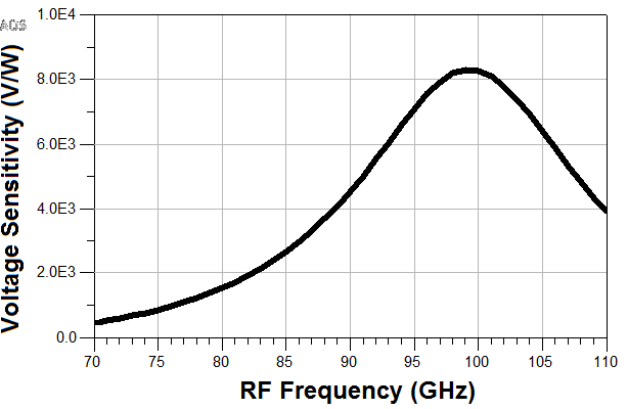
CHAPTER 7
154
The next step for the simulation was to set the input power to -29 dBm, and sweep the
input frequency. As can be seen in Figure 7.12, the peak sensitivity is 8300 V/W at 98 GHz
(slightly lower than target of 100 GHz), this is due to the matching circuit not being
exactly matched at 100 GHz. However, this mismatch only had a very minor effect on the
sensitivity which changed from 8300 to 8260 V/W.
Figure 7.12 Voltage sensitivity of 4×4 μm² InGaAs-AlAs ASPAT diode with respect of input
RF frequency (100 GHz)
7.6.3.2 240 GHz InGaAs-AlAs ASPAT detector simulation
The other detector circuit using a 4×4 μm² InGaAs-AlAs ASPAT diode was designed to
work at 240 GHz. By using the same design method, and redefined the matching circuits,
the transfer functions and voltage sensitivity of the 4×4 μm² InGaAs-AlAs ASPAT diode
at 240 GHz were obtained as depicted in Figure 7.13 The output voltage starts to saturate
when the applied input power was higher than -4 dBm.

CHAPTER 7
155
Figure 7.13 Transfer functions of 4×4 μm² InGaAs-AlAs ASPAT diode at 240 GHz
Sweeping the input power, the highest simulated voltage sensitivity achieved at 240 GHz
was 1340 V/W when the input power was -21 dBm.
Figure 7.14 Voltage sensitivity of 4×4 μm² InGaAs-AlAs ASPAT diode at 240 GHz as a
function of input power
The input power was then fixed to -21 dBm and the signal frequency swept from 210 GHz
to 270 GHz. The highest sensitivity was 1410 V/W which was achieved at 235 GHz. The
shift of the peak value is due to the mismatch of the matching circuit. At the design
frequency 240 GHz, the voltage sensitivity was 1390 V/W, which is almost the same as the
peak value.

CHAPTER 7
156
Figure 7.15 Voltage sensitivity of 4×4 μm² InGaAs-AlAs ASPAT diode with respect of input
RF frequency (240 GHz)
7.6.3.3 Detector performance comparisons between SBDs and InGaAs-AlAs ASPAT
diode
Comparing with the commonly used SBDs, the simulated results show that the InGaAs-
AlAs ASPAT diode has promising potential in high frequency detection. The detailed
voltage sensitivity/responsivity comparisons of various devices reported in the literature
and operating in the 100 GHz and 250 GHz regions are listed in Table 7-2.
When the operating frequency is around 100 GHz, the simulated peak sensitivity of the
InGaAs-AlAs ASPAT diode is 8300 V/W (at 98 GHz), which is much higher than some
commoditised SBDs and reported results listed in Table 7-2.
In the range around 240 GHz, the peak voltage sensitivity of the InGaAs-AlAs ASPAT
diode is around 1410V/W, this was also comparable with the best reported responsivity of
the SBDs.

CHAPTER 7
157
Table 7-2 Comparisons of SBDs and InGaAs-AlAs ASPAT detectors
Detector
Type
Operation
frequency (GHz)
Responsivity
(V/W)
Peak
Responsivity
(V/W)
References
Schottky
89
896
-
[175]
100
~400
-
[176]
100
4000
-
[177]
100
3800
-
[175]
110-170
2000
-
[178]
ASPAT(this
work)
93-106
>6000
8300 @98GHz
Schottky
200
900
-
[176]
200
1900
-
[175]
250
430
-
[179]
250
1080
-
[176]
280
336
-
[180]
ASPAT(this
work)
217-254
>1300
1410@235GHz
In addition, the voltage sensitivity drift with temperature of the SBDs has been reported
[175]. The results showed that for the same SBDs, the responsivity dropped from 3800 to
3000 V/W when the operation temperature decreased from 40 ºC to room temperature at
100 GHz, and fell from 2000 to 1800 V/W at 200 GHz. In the case of InGaAs-AlAs
ASPAT diodes, as the temperature dependence measurements showed in Chapter five, the
I-V characteristics changed only very little over large temperature ranges. Take the
detector circuit operating at 100 GHz as an example. The simulated voltage sensitivity of

CHAPTER 7
158
the InGaAs-AlAs ASPAT at 350 K is shown in Figure 7.16. In this simulation, the
matching circuits were kept the same as they were at room temperature.
When comparing with the sensitivity achieved at room temperature, the peak value which
was 8180 V/W only changed by 120 V/W (1.5%). This drop was due to mismatching with
the matching circuits and the junction resistance decreased as the current slightly increased.
With a larger temperature range (50 K), this change was much smaller than it is for the
SBDs which dropped by 27%. Thus two conclusions can be made. The first is that the
responsivity of the InGaAs-AlAs ASPAT detector was almost the same as its room
temperature value. The second is the circuit temperature performance, with the InGaAs-
AlAs ASPAT diode more stable than SBDs. Thus, this temperature stability property can
lead the InGaAs-AlAs ASPAT detector to be used in a much wider applicable temperature
range without the need for temperature compensation circuitry.
Figure 7.16 Voltage sensitivity of 4×4 μm² InGaAs-AlAs ASPAT diode with respect of input
RF frequency (350 K)
However, note that all the responsivities of the InGaAs-AlAs ASPAT detectors were
simulated values and not experimental ones (even though the design of the detector circuits
was based on real, fabricated ASPAT devices). In the simulation, all the designs, such as
matching designs and the other lumped components, were set under perfect conditions. For
future work, a mask layout based on these simulations will be designed and fabricated
detector circuits measured to calibrate the simulated models.
CHAPTER 7
159
7.7 Summary
This chapter focuses on the AC performances of ASPAT diode. The junction capacitances,
diode conductance and the S-parameters of both GaAs-AlAs and InGaAs-AlAs ASPAT
diodes were obtained, for the first time, from SILVACO AC simulations. The junction
capacitance and S-parameters showed excellent fits with measurements. The equivalent
circuit of the InGaAs-AlAs ASPAT diode were then extracted taking into account proper
de-embedding methods. By using the parameters extracted from the equivalent circuit, 100
GHz and 240 GHz zero bias InGaAs-AlAs ASPAT detector circuits were designed. The
simulated voltage sensitivity of InGaAs-AlAs ASPAT detector was 1.5 times higher than
that of the SBDs at 100 GHz, and 1.2 times higher at 250 GHz. The simulated results
showed that the InGaAs-AlAs ASPAT detectors had higher voltage sensitivities for
operations at both frequencies. In addition, the comparison of the voltage sensitivity at
room temperature and 350 K proved that the diode performance was much more stable
than a SBD. When compared with SBDs, the temperature insensitive property of the
InGaAs-AlAs ASPAT diode makes it a more stable and efficient RF device under a wide
range of operating temperatures.
CHAPTER 8
160
CHAPTER 8: CONCLUSIONS AND FUTURE WORK
The final Chapter of this thesis provides a brief summary of the work presented in
Chapters 4 through 7, together with the main conclusions. The ideas and directions of
future work are also given in this chapter.
8.1 Conclusions
The work in this thesis detailed an extensive and in-depth study of semiconductor tunnel
diodes and photoconductive switches to investigate both optical and electronic approaches
to THz generation and detection.
For the optical approach, optimised THz photoconductive devices based on III-V
semiconductor grown at low temperature conditions using Molecular Beam Epitaxy were
investigated. The optical and transport properties as well as the TDS characteristics of
these photoconductive samples operating at excitation wavelengths of 800 nm and 1.55 µm
were studied. The effect of coupling the DBR layers with the active layers of
photoconductors were compared with the base line efficient photoconductors. The results
showed that the DBR layers did not affect the mobility and the resistivity of the
photoconductive materials and the reflectivity of DBRs at the desired wavelengths (800nm
and 1.55 µm) were matched with the designed structures. In the TDS testing, LT GaAs
optimised photoconductive switches based system had responses with THz pulses having
power up to 4 THz and dynamic range of 60 dB or more, while the LT InGaAs-InAlAs
optimised photoconductive switches based system had responses with power up to 2.5 THz
and with 50 dB noise floor. For both optimised LT GaAs and LT InGaAs-InAlAs switches,
coupling DBRs layers also results in an increase of the transmitter photocurrent, a marked
enhancement of the THz peak signal (more than twice), and a doubling of the optical to
electrical efficiency. Thus, the performances of these optimised photoconductive switches
excited at 800 nm and 1.55 µm show better performances and allow for higher quality THz
applications to be investigated.
Our main industrial partner (TeTechs) commercialises switches (incorporating our devices)
and operating at 800 nm and 1.55 µm by mounting the photoconductive antennas into THz
modules with a hyper-hemispherical silicon lens and an SMA connector. In addition, the
collaboration also resulted in the Rigel 1550 Spectrometer which is an innovative low cost,
CHAPTER 8
161
portable, room temperature operated and reconfigurable fiber coupled THz spectrometer.
The beam delivery part is independent of the laser and can be easily connected to any
femtosecond laser at telecom wavelength. By using the Rigel 1550 Spectrometer, the
transparencies of a series of materials were obtained. From these measurements, SI InP and
SI GaAs substrate of the structures operating at excitation wavelengths of 800 nm and 1.55
µm were found to be transparent to the signal in the THz frequency range. Thus, there is no
need to remove the substrates as they do not affect the generation of THz radiation. This
further allows the photoconductive antennas to be low cost and high yielding devices.
Objects such as cotton clothes and paper were also transparent to THz signals suggesting
potential THz application in security checking. In addition, the associated absorption
spectrum of a bunch of paper also showed good agreement with the absorption lines of
water vapor. THz measurements on biological sample objects such as leaves and a human
hand were also made and showed the potential for interdisciplinary between biological
research and THz technology. In the future, this spectrometer will benefit the University of
Manchester for medical, biological and other fields for as yet untapped THz properties.
For the electronic approach, a new type of InP-based Asymmetric Spacer Tunnel Diode
(ASPAT) was investigated. The growth of the material was performed using molecular
beam epitaxy (MBE) which can control very precisely the thickness of active layers
(especially barrier) of the ASPAT down to a fraction of a monolayer. A key novelty in the
SI InP based ASPAT studied here is the replacement of conventional GaAs with
In
0.53
Ga
0.47
As. This produced a larger band discontinuity from spacer to barrier, thus
ensuring tunnelling to be dominant rather than thermionic emission in the transport
mechanisms.
The InGaAs-AlAs ASPAT diodes were designed to be used as zero bias detectors at high
frequencies. The asymmetric InGaAs spacers sandwiching the AlAs barrier contributed to
the asymmetric I-V characteristics and made this diode have a nonlinear region which is
essential for detection.
This project dedicated efforts to not only mask designs and layouts but also developed
optimised processes to achieved state of the art high-frequency performances from the
fabricated devices. To simultaneously measure both DC and high frequency characteristics
of the devices, the mask layout was designed to use a ground-signal-ground (GSG) contact
structure with optimised strip width. An optimised process combining both wet and dry
CHAPTER 8
162
etching methods was also developed. As the device was designed to use an air-bridge
technique, this unique combination method with a precisely controlled time was used to
achieve anisotropic etching and successful opening of the air-bridge to make small device
mesa area and to allow the device to work at high frequencies.
After successful fabrication, the temperature dependence of the InGaAs-AlAs ASPAT
diode was investigated and its I-V characteristics measured at various temperatures and
compared with those of a Schottky diode (SBD) and a conventional GaAs-AlAs ASPAT
diode respectively. These comparisons illustrate that the ASPAT diode’s characteristics
have only a minor residual temperature dependence compared with SBDs and the currents
in the InGaAs-AlAs ASPAT only marginally changed over the temperature range of 77K
to 400K. When compared with the conventional GaAs-AlAs ASPAT, the new design
showed an even better temperature stability due to its relatively higher barrier height. This
property allows this type of diode to stably operate over a very wide range of temperature.
In addition, physical modelling of this new type of ASPAT diode was developed. This
physical device simulation helped to give insight into the physics of this new zero bias
detectors. The diode DC characterises can be simulated not only at room temperature, but
also at various temperatures, and all simulated results showed excellent matching with
measurements. The band diagram of the InGaAs-AlAs ASPAT showed a much higher
conduction band discontinuity (around 0.5 eV) compared to that of GaAs-AlAs ASPAT
diodes, thus the height of the barrier to electron transport is larger. This higher barrier
limits even further the thermionic transport of elections and hence tunneling is the
dominant mechanism in InGaAs-AlAs ASPAT. The simulation also helped to confirm that
the properties of InGaAs-AlAs ASAPT diode lead to a much more temperature insensitive
diode behaviour.
After successfully developing the DC model of ASPAT diode, the AC performances were
extracted from SILVACO AC models. The junction capacitance, conductance and S-
parameters of the intrinsic InGaAs-AlAs ASPAT diode were obtained. By using the ADS
empirical model, the SILVACO simulated S-parameter results showed excellent matching
with the RF measurements. From the RF measurements, the equivalent circuit which
consists of the series resistance, junction capacitance and junction resistance of the
InGaAs-AlAs ASPAT diodes can be extracted. At zero bias, the simulated junction
capacitance of a 4×4 μm² InGaAs-AlAs ASPAT diode was found to be 18 fF which was
CHAPTER 8
163
identical to the extracted value from the equivalent circuit and RF measurements. The
detector circuit using 4×4 μm² devices for 100 GHz and 240 GHz detections were designed.
These simulated results showed higher voltage sensitives than those of SBDs at both
frequencies. In addition, from a simulation for the InGaAs-AlAs ASPAT detector at an
operation temperature at 350 K, the simulated sensitivity only dropped by 120 V/W ( ~ 1.5%
change) over the 50 K temperature change while the change for the SBD was 800 V/W
(27%) over 10 K temperature variations.
8.2 Further Work
This short section will suggest a number of new approaches to further improve the high
frequency of devices
8.2.1 Photoconductive switches
By adding distributed Bragg reflector (DBR) layers below the active layers, optimised
photoconductive materials excited at 800 nm and 1.55 µm can further improve the already
efficient performance of the photoconductor. It is however worth checking the
performance of these switches in continuous wave (CW) operating system. Such studies
will bring the prospects for a truly portable and high efficient THz imaging system much
closer to reality.
The Rigel 1550 Spectrometer has enormous potential and can also be extended to benefit
different schools on the University of Manchester with collaborations with medical,
biological, chemistry and other schools.
8.2.2 InGaAs-AlAs ASPAT diode
The key investigations of this newly designed InGaAs-AlAs ASPAT diode have been
demonstrated in this work. The DC characteristics from 77 K to 400 K were studied and
compared with SBDs and conventional GaAs-AlAs ASPAT diode. In addition, the RF
performances of this type of ASPAT have been measured up to 40 GHz. The 100 GHz and
240 GHz zero bias detector circuit based on measured diode characteristics (4×4 μm²
devices) were designed and their performances simulated.
This is the first attempt at RF design of complete receiver circuit, growth, fabrication and
testing of InGaAs-AlAs ASPAT diodes. For further work, more wafers using the various
CHAPTER 8
164
optimisations are worth growing and fabricating. Compared with the conventional design,
InGaAs-AlAs ASPAT has a 0.5 eV higher barrier height making it a far more efficient
tunnel device.
In order to work at even higher frequencies, devices with even smaller mesa sizes are
needed. In addition, the mask schematic layout based on the detector circuit simulation
should be fabricated and RF performances of fabricated circuits investigated. Furthermore,
the integration of the detector with an antenna structure can be the next step for realising
compact zero bias, zero power dissipating millimetre-wave and THz devices. Beyond these,
the ASPAT can also be used for many other applications such as high-frequency mixers
and multipliers. These will bring the ASPAT diode based applications one step closer to
reality and make it an essential component of massive connectivity in the internet of thing
(IoT) deployments.
APPENDIX
165
APPENDIX
Appendix A1: The preparation of Hall Effect samples
1. Cleave the sample in 7.5 mm × 7.5 mm size
2. Clean sample with NMP (1165) and DI Water and dry with N
2
3. Spin a layer of photoresist S1805, Time = 30 sec
4. Prebake in hotplate at 115 °C for 1 min
5. Place the metallic cloverleaf pattern on the sample and exposure using UV Eraser for 10
mins
6. Develop using MF319 for 2 mins, rinse with DI water and dry with N
2
7. Post bake in hotplate at 120 °C for 5 mins to harden the resist before etch
8. Etch using Ortho-phosphoric (3:1:50 of H
3
PO
4
:H
2
O
2
:H
2
O) for 15 mins
9. Clean the sample with Acetone / IPA and dry with N
2
to remove the resist
10. Place four small cubic dots of pure Indium on the four square corners of the formed
cloverleaf pattern
11. Anneal at 310 °C for 3 mins (InGaAs-InAlAs Samples) / 420 °C for 3 mins (GaAs
Samples) under N
2
flow using the alloying jig

APPENDIX
166
Appendix A2: The fabrication process of photoconductive antennas
MESA
Sample cleaning
NMP for 5 mins and Dry with N
2
Preheat in hotplate at 120 °C for 5 mins
Resist coating
S1805 for 30 sec
Prebake in hotplate at 120 °C for 1 min
Photolithography
Align the mesa mask and exposure for 20 sec (0.9mW i-
line)
Develop in MF 319 for 1 min, rinse with DI water and
dry with N
2
Post bake in hotplate at 120 °C for 5 mins
Etching
Calibration, etch calibrated sample for 20 sec using
Orthophosphoric (H
3
PO
4
:H
2
O
2
:H
2
O=2:1:2)
Calculate the etching time by considering the mesa
height
Sample cleaning
Clean the sample with Acetone / IPA, dry with N
2

APPENDIX
167
OHMICS
Sample cleaning
NMP for 5 mins and Dry with N
2
Preheat in hotplate at 120 °C for 5 mins
Resist coating
AZnLOF (2μm) for 30 sec
Prebake in hotplate at 110 °C for 1 min
Photolithography
Align the mesa mask and exposure for 5.5 sec
Post Exposure bake at 110 °C for 1 min
Develop in MF 326 for 1 min, rinse with DI water and
dry with N
2
Metallisation
Clean with HCL (HCL:H
2
O=1:1) for 1min
Evaporate 2 cm Ti (50 nm) and 5.5 cm (150 nm) Au
using thermal evaporator
Lift-off
Place the sample in NMP for 40 mins at room
temperature
Clean the sample with Acetone / IPA, dry with N
2
Annealing
Anneal the contacts at 250 °C for 1 min under N
2
flow
using the alloying jig

APPENDIX
168
Appendix A3: The fabrication process of GaAs-AlAs ASPAT diodes
OHMICS (TOP CONTACTS)
Sample cleaning
NMP for 5 mins and Dry with N
2
Preheat in hotplate at 120 °C for 5 mins
Resist coating
Spin AZnLOF (0.5μm) for 30 sec
Prebake in hotplate at 110 °C for 1 min
Photolithography
Align the mesa mask and exposure for 12sec (0.9mW i-
line)
Post Exposure bake at 110 °C for 1 min
Develop in MF 326 for 1 min, rinse with DI water and
dry with N
2
Metallisation
Clean with HCL (HCL:H
2
O=1:1) for 1min
Evaporate AuGe (100 mg), Ni (1.0 cm) and Au (15 cm)
using thermal evaporator
Lift-off
Place the sample in NMP for 40 mins at room
temperature
Clean the sample with Acetone / IPA, dry with N
2

APPENDIX
169
MESA (ISOLATION)
Sample cleaning
NMP for 5 mins and Dry with N
2
Preheat in hotplate at 120 °C for 5 mins
Resist coating
Spin S1813 for 30 sec
Prebake in hotplate at 120 °C for 1 min
Photolithography
Align the mesa mask and exposure for 2 mins (0.9mW i-
line)
Develop in MF 319 for 1 min, rinse with DI water and
dry with N
2
Post bake in hotplate at 120 °C for 5 mins
Etching
Calibration, etch calibrated sample for 2 mins using
Orthophosphoric (H
3
PO
4
:H
2
O
2
:H
2
O=3:1:50)
Calculate the etching time by considering the mesa
height
Sample cleaning
Clean the sample with Acetone / IPA, dry with N
2

APPENDIX
170
MESA (MESA ETCH)
Sample cleaning
NMP for 5 mins and Dry with N
2
Preheat in hotplate at 120 °C for 5 mins
Resist coating
S1805 for 30 sec
Prebake in hotplate at 120 °C for 1 min
Photolithography
Align the mesa mask and exposure for 20 sec (0.9mW i-
line)
Develop in MF 319 for 1 min, rinse with DI water and
dry with N
2
Post bake in hotplate at 120 °C for 5 mins
Etching
Calibration, etch calibrated sample for 20 sec using
Orthophosphoric (H
3
PO
4
:H
2
O
2
:H
2
O=2:1:2 and 3:1:50)
Calculate the etching time by considering the mesa
height
Sample cleaning
Clean the sample with Acetone / IPA, dry with N
2

APPENDIX
171
BOTTOM CONTACTS
Sample cleaning
NMP for 5 mins and Dry with N
2
Preheat in hotplate at 120 °C for 5 mins
Resist coating
AZnLOF (2 μm) for 30 sec
Prebake in hotplate at 110 °C for 1 min
Photolithography
Align the mesa mask and exposure for 5.5 sec (0.9mW i-
line)
Post Exposure bake at 110 °C for 1 min
Develop in MF 326 for 1 min, rinse with DI water and
dry with N
2
Metallisation
Clean with HCL (HCL:H
2
O=1:1) for 1min
Evaporate AuGe (100 mg) and Au (15 cm) using thermal
evaporator
Lift-off
Place the sample in NMP for 40 mins at room
temperature
Clean the sample with Acetone / IPA, dry with N
2
Annealing
Anneal the contacts at 420 °C for 2 mins under N
2
flow
using furnace

APPENDIX
172
DIELECTRIC LAYER
Sample cleaning
NMP for 5mins and Dry with N
2
Preheat in hotplate at 120 °C for 5 mins
Resist coating
S1805 for 30 sec
Prebake in hotplate at 120 °C for 1 min
Photolithography
Align the mesa mask and exposure for 20 sec (0.9mW i-
line)
Develop in MF 319 for 1 min, rinse with DI water and
dry with N
2
Hard bake in hotplate at 250 °C for 30 mins

APPENDIX
173
DIELECTRIC BRIDGE
Sample cleaning
NMP for 5mins and Dry with N
2
Preheat in hotplate at 120 °C for 5 mins
Resist coating
AZnLOF (2μm) for 30 sec
Prebake in hotplate at 110 °C for 1 min
Photolithography
Align the mesa mask and exposure for 5.5 sec (0.9mW i-
line)
Post Exposure bake at 110 °C for 1 min
Develop in MF 326 for 1 min, rinse with DI water and
dry with N
2
Metallisation
Clean with HCL (HCL:H
2
O=1:1) for 1min
Evaporate Ti (1cm) and Au (15 cm) using thermal
evaporator
Lift-off
Place the sample in NMP for 40 mins at room
temperature
Clean the sample with Acetone / IPA, dry with N
2

APPENDIX
174
Appendix A4: The fabrication process of InGaAs-AlAs ASPAT diodes
OHMICS (TOP CONTACTS)
Sample cleaning
NMP for 5 mins and Dry with N
2
Preheat in hotplate at 120 °C for 5 mins
Resist coating
Spin AZnLOF (0.5μm) for 30 sec
Prebake in hotplate at 110 °C for 1 min
Photolithography
Align the mesa mask and exposure for 12 sec (0.9mW i-
line)
Post Exposure bake at 110 °C for 1 min
Develop in MF 326 for 1 min, rinse with DI water and
dry with N
2
Metallisation
Clean with HCL (HCL:H
2
O=1:1) for 1 min
Evaporate Ti (1 cm) and Au (15 cm) using thermal
evaporator
Lift-off
Place the sample in NMP for 40 mins at room
temperature
Clean the sample with Acetone / IPA, dry with N
2

APPENDIX
175
MESA (ISOLATION)
Sample cleaning
NMP for 5 mins and Dry with N
2
Preheat in hotplate at 120 °C for 5 mins
Resist coating
Spin S1813 for 30 sec
Prebake in hotplate at 120 °C for 1 min
Photolithography
Align the mesa mask and exposure for 2 mins (0.9mW i-
line)
Develop in MF 319 for 1 min, rinse with DI water and
dry with N
2
Post bake in hotplate at 120 °C for 5 mins
Etching
Calibration, etch calibrated sample for 2 mins using
Orthophosphoric (H
3
PO
4
:H
2
O
2
:H
2
O=3:1:50)
Calculate the etching time by considering the mesa
height
Sample cleaning
Clean the sample with Acetone / IPA, dry with N
2

APPENDIX
176
MESA (MESA ETCH)
Sample cleaning
NMP for 5 mins and Dry with N
2
Preheat in hotplate at 120 °C for 5 mins
Resist coating
Spin S1805 for 30 sec
Prebake in hotplate at 120 °C for 1 min
Photolithography
Align the mesa mask and exposure for 20 sec (0.9mW i-
line)
Develop in MF 319 for 1 min, rinse with DI water and
dry with N
2
Post bake in hotplate at 120 °C for 5 mins
Etching
Calibration, etch calibrated sample for 10mins using dry
etching method (CH
4
and H
2
) 10 mins, and O
2
polymer
removal for 10mins
Calculate the etching time by considering the mesa
height
Sample cleaning
Clean the sample with Acetone / IPA, dry with N
2

APPENDIX
177
MESA (AIR BRIDGE OPENING)
Sample cleaning
NMP for 5 mins and Dry with N
2
Preheat in hotplate at 120 °C for 5 mins
Resist coating
Spin S1805 for 30 sec
Prebake in hotplate at 120 °C for 1 min
Photolithography
Align the mesa mask and exposure for 20 sec (0.9mW i-
line)
Develop in MF 319 for 1 min, rinse with DI water and
dry with N
2
Post bake in hotplate at 120 °C for 5 mins
Etching
Calibration, check the test structures to extracted the
undercut ratio (H
3
PO
4
:H
2
O
2
:H
2
O=3:1:50)
Calculate the etching time by considering the undercut
ratio
Sample cleaning
Clean the sample with Acetone / IPA, dry with N
2

APPENDIX
178
BOTTOM CONTACTS AND BOND PAD
Sample cleaning
NMP for 5 mins and Dry with N
2
Preheat in hotplate at 120 °C for 5 mins
Resist coating
AZnLOF (2μm) for 30 sec
Prebake in hotplate at 110 °C for 1 min
Photolithography
Align the mesa mask and exposure for 5.5 sec (0.9mW i-
line)
Post Exposure bake at 110 °C for 1 min
Develop in MF 326 for 1 min, rinse with DI water and
dry with N
2
Metallisation
Clean with HCL (HCL:H
2
O=1:1) for 1min
Evaporate Ti (1cm) and Au (15cm) using thermal
evaporator
Lift-off
Place the sample in NMP for 40 mins at room
temperature
Clean the sample with Acetone / IPA, dry with N
2
Annealing
Anneal the contacts at 280 °C for 2 mins under N
2
flow
using furnace

APPENDIX
179
Appendix B: The instruction of the Rigel 1550 THz spectrometer
Figure B1shows the Rigel 1550 THz spectrometer.
Figure B 1 Photo of Rigel 1550 THz spectrometer
The main body of the spectrometer is only 70 cm×50 cm×90 cm. All the key elements are
shown in Figure B2 and listed in Table B-1.

APPENDIX
180
(a)
(b) (c)
Figure B 2 Photo of Rigel 1550 THz spectrometer (a) sensor heads
(b) front panel and (c) back panel
Table B-1 Key elements of Rigel 1550 THz spectrometer (respects to number in Figure B 2)
Numbers respect
to Figure B1
Component
1
Optical Delay module
2
Onefive ORIGAMI Femtosecond Laser
3
Shaker electronic controller
4
Laser driver
5
Linear stage for slow scan
6
Lock-in amplifier
7
NI DAQ for data acquisition
8
Square wave generator
9
USB Hub
10
Shaker power supply
APPENDIX
181
The different optical delay scan units allow the adjusted distance between photoconcdutive
modules to be up to 1 metre, making the system capable of characterising samples under
different situations. The plano-convex lenses also help collimate the THz beam easily onto
the samples under test.
The experimental procedure steps for the Rigel 1550 THz spectrometer are as follows:
i. Connection checking: Before turning on the PC and spectrometer, the
connection of the transmitter and the receiver must be checked. The connection
of the USB from PC to the spectrometer cabinet for electrical components must
be in position.
ii. Self-test: In this step, the interface between PC and spectrometer is checked by
using NI-DAQ driver version 9.3.
iii. Shaker moving: Run Shaker.exe until the serve position goes to the center and
activates the shaker to be in the middle position.
iv. Align: Run Show_Signal.exe and adjust the position of transmitter and detector.
By doing this, stronger THz signal can be achieved.
v. Setting: under the setting options, click ‘Go Home’ every time before each scan.
This signals to the software that a new run is going to begin.
vi. Scan: set start position to 2 mm, motor speed to 0.1 mm/s. The scan width for
Rigel 1550 THz spectrometer is up to 50 mm, after setting these parameters, the
stop position can be automatically calculated by Rigel.exe.

APPENDIX
182
Appendix C: Introduction and specification of SILVACO
As shown in Figure C1, ATLAS simulation allows two kinds of inputs: the structure files
which contain definitions of the structure and the text file using syntax commands to allow
ATLAS to execute. The input part allows users to define/model structure, materials and the
physical characteristics of the designed devices. Three types of output are provided by
ATLAS. The runtime output, where the warning and error messages are shown, illustrates
the progress of simulations. Log files act as the storage for all terminal information from
the device analysis and the solution files store two or three-dimensional data of the solution
variables of the device. The simulated data of the process contains the numerical and
model analysis of the device and these results are then plotted by the visualization tool
called TonyPlot.
Figure C 1 ATLAS inputs and output [166]
Simulations follow the same process independently of the specific information of devices.
The general steps of SILVACO simulation are shown in Figure C 2.

APPENDIX
183
Figure C 2 ATLAS command group [166]
Structure specification
(1) Mesh
Mesh statement works to define the two or three dimensional Cartesian grids of the
structure. The default unit for all coordinates is micrometer to improve the accuracy and
precision of the analysis.
The mesh should be carefully defined throughout the device structure. For example, the
main part which includes the area slightly before and after the AlAs barrier in the ASPAT
structure, needs to be set to more points in order to achieve accurate calculations. The
device mesh structure for InGaAs-AlAs ASPAT diode with a mesa size of 4×4 µm
2
is
shown in Figure C 3.
Structure
Specification
• Mesh
• Region
• Electrode
Material
Models
Specification
• Material
• Models
• Contact
• Interface
Numerical
Method
Selection
• Method
Solution
Specification
• Log
• Solve
• Load
• Save
Results
Analysis
• Extract
• Tonyplot

APPENDIX
184
Figure C 3 Device mesh structure for InGaAs-AlAs ASPAT with a mesa size of 4×4 µm
2
(2) Region
Region statement is used to define the isolated location of the device. By using ‘Region’,
the initial mesh statement is separated into distinct blocks. The material parameters of each
block will be set by the referred region number. The region number must be ordered from
the lowest to highest region and mesh must be assigned to a region.
(3) Electrode
The next statement after defining the device region is electrode. Electrodes need to be
defined on the selected device area for electrical analysis. The following syntax is the
electrodes define statements used in this work:
#electrodes
Electrode name=anode top
Electrode name=cathode bottom
Material Models Specification
APPENDIX
185
(1) Materials
Material is associated with physical parameters with materials in the mesh. In ATLAS, all
the default parameters are set for silicon properties as SILVACO was first developed for
Silicon based devices. However, users are able to define materials such as GaAs, InGaAs,
InAlAs, etc. with the pre-established names in the region statements. Normally, the user-
defined material parameters are required especially for their energy band bap, effective
masses, permittivity, and effective density of states etc. It is important that all required
parameters are checked and clearly defined in the section material parameters; it is also
necessary to check parameters which are required in the correspond models. This is
because that if the required parameters are not defined in this statement, SILVACO will
automatically use the default Silicon parameter instead.
(2) Models
Models used in SILVACO refer to the physical equations used in the device analysis. In
order to accurately simulate the device, model statements need to be carefully chosen to
specify the particular phenomenon otherwise it will require different mathematical models,
and physical mechanisms.
(3) Contact
The purpose of defining the contact statement is to specify the physical attribute of the
electrodes. In SILVACO, the default for the metal-semiconductor is the perfect Ohmic
contact. The name of contact is used to identify each electrode property.
(4) Numerical methods selection
Methods are used to discretise the problem and then estimate the solution. There are three
different numerical methods available in ATLAS which can be used to solve the
semiconductor device equations.
“Newton” is widely used for linearizing the non-linear problem. In Newton, all
unknowns are put together to solve the total system. Users should be careful in
defining the mesh since the wrong definition of mesh will cause Newton to fail to
converge. Compared to other methods, Newton usually converges since it
automatically adjusts the step size to find the solution, but as a result takes a longer
processing time.
APPENDIX
186
“Gummel” is a decoupled numerical method to solve each unknown in turn keeping
all other variables as constant. It is useful to the system with equations weakly
coupled and only works for linear convergence. In order to avoid non-convergence,
Gummel will truncate the over range results.
“Block” is a method which is able to produce a quick simulation, but at the expense
of accuracy compared to the other two methods. This method is recommended for
devices that require analysis of energy balance and lattice heating.
Generally, the simulation can first choose to use the Gummel method then switch to
Newton to complete the solution. These numerical methods specifications are provided in
the method statements of the input file. For ASPAT diodes, Newton method is used to
achieve faster converges compared with Gummel, but requires a longer calculation time
per step.
(5) Solution specification
To obtain solutions, SOLVE must be invoked. At the start of the solution statement,
SOLVE INIT can make the first solution under equilibrium conditions. Users need to
define voltages on the electrode defined previously in the structure specification. The bias
steps need to be well defined to obtain the desired results accuracy and reduce the
processing time.
(6) Results stored
Log files are used to obtain and store the results and these results are plotted by “TonyPlot”.
The plotted results can be then exported to other file types. In the case of the ASPAT diode
simulation code, the log file includes the DC or AC data generated by the solve statement.
APPENDIX
187
Appendix D: The DC simulation code of InGaAs-AlAs ASPAT diodes
GO ATLAS
# Thicknesses
#---------------------------------------------------------
#Structure parameter definition (Constants) values in 'um'
#---------------------------------------------------------
## Thicknesses
set t_contact1=0.1
set t_ohmic1=0.3
set t_emitter=0.035
set t_spacer1=0.005
set t_barrier=0.00283
set t_spacer2=0.2
set t_collector=0.035
set t_ohmic2=0.4
set t_etch=0
set t_contact2=0.1
## Doping concentrations
set d_ohmic1=1.5e19
set d_emitter=1e17
set d_collector=1e17
set d_ohmic2=1.5e19
set d_gap=1.5
set d_mesa=7.9
set d_device=20
## Layers
APPENDIX
188
set I=$t_contact1
set A=$I+$t_ohmic1
set B=$A+$t_emitter
set C=$B+$t_spacer1
set D=$C+$t_barrier
set E=$D+$t_spacer2
set F=$E+$t_collector
set G=$F+$t_ohmic2
#-------------------------------------
# Mesh generator
#-------------------------------------
## The x.mesh and y.mesh specifies the location 'loc' of mesh grid lines along the
respective
## axis. 'spacing' determines the mesh spacing in microns at the position specified by 'loc'
## parameter. The mesh spacing from one mesh statement to the next is gradually changed
and is managed by the simulator itself.
mesh diag.flip width=8
x.mesh location=0 s=0.5
x.mesh location=$d_mesa s=0.5
x.mesh location=$d_device s=0.5
# Ohmic1
y.mesh l=0.000 s=0.005
y.mesh l=$I s=0.005
y.mesh l=$A s=0.005
y.mesh l=$B s=0.005
y.mesh l=$C s=0.003
y.mesh l=$D s=0.0001
APPENDIX
189
y.mesh l=$E s=0.005
y.mesh l=$F s=0.005
y.mesh l=$G s=0.005
#-----------------------------------
# SECTION 2: Structure Specification
#-----------------------------------
#-----------------------------------
# Regions definition
#-----------------------------------
region num=1 name=contact1 material=Gold y.min=0 y.max=$I
region num=2 name=ohmic1 material=InGaAs x.comp=0.47 y.min=$I y.max=$A
region num=3 name=emitter material=InGaAs x.comp=0.47 y.min=$A y.max=$B
region num=4 name=spacer1 material=InGaAs x.comp=0.47 y.min=$B y.max=$C
region num=5 name=barrier material=AlAs y.min=$C y.max=$D x.min=0
x.max=$d_mesa calc.strain qtregion=1
region num=6 name=spacer2 material=InGaAs x.comp=0.47 y.min=$D y.max=$E
region num=7 name=collector material=InGaAs x.comp=0.47 y.min=$E y.max=$F
region num=8 name=ohmic2 material=InGaAs x.comp=0.47 y.min=$F y.max=$G
region num=10 name=etch material=Air y.min=0 y.max=$F+$t_etch x.min=$d_mesa
x.max=$d_device
#---------------------------------
# Electrodes
#---------------------------------
electrode num=1 name=anode x.min=0 x.max=$d_mesa y.min=0 y.max=$I material=Gold
electrode num=2 name=cathode x.min=$d_mesa+$d_gap x.max=$d_device
y.min=$F+$t_etch-$t_contact2 y.max=$F+$t_etch material=Gold
#--------------------------------
APPENDIX
190
# Doping
#--------------------------------
doping uniform n.type conc=$d_ohmic1 Region=2
doping uniform n.type conc=$d_emitter Region=3
doping uniform n.type conc=$d_collector Region=7
doping uniform n.type conc=$d_ohmic2 Region=8
#--------------------------
#Interface
#--------------------------
interface s.c y.min=$I y.max=$I
interface s.s y.min=$A y.max=$A
interface s.s y.min=$B y.max=$B
interface s.i y.min=$C y.max=$C
interface s.i y.min=$D y.max=$D
interface s.s y.min=$E y.max=$E
interface s.s y.min=$F y.max=$F
interface s.c y.min=$F+$t_etch y.max=$F+$t_etch x.min=$d_mesa+$d_gap
x.max=$d_device
interface tunnel region=5 dy.tunnel=0.001
#--------------------------
#Contacts
#--------------------------
contact name=cathode
contact name=anode
#------------------------------------------
# SECTION 3: Material & Models Definitions
APPENDIX
191
#------------------------------------------
## The physical parameters for the materials are defined in the following three sub-
sections
#AlAs
material material=AlAs eg300=2.83 affinity=3.5
# align=0.684
#InGaAs x.comp=0.47
material material=InGaAs permittivity=13.876 eg300=0.74 affinity=4.51 nc300=1.55e18
########INITIAL BAND DIAGRAM ####
output t.quantum band.param qfn qfp val.band con.band charge polar.charge flowlines
solve init
save outf=XMBE326_INITIAL.str
tonyplot XMBE326_INITIAL.str
#------------------------------------------
###### ANALYSIS #####
#------------------------------------------
models sis.el sis.ho sis.nlderivs qtregion=1 print
inttrap acceptor structure=top e.level=0.2 density=3.5e11 degen.fac=1 sign=1e-19
sigp=1e-17
#########################################################################
#####################
#DC ANALYSIS
#########################################################################
#####################
log outf=XMBE326_BIASED.log
solve init
solve vanode=-1.5 name=anode vstep=0.01 vfinal=1.5
APPENDIX
192
save outf=XMBE326_BIASED.str
log off
tonyplot XMBE326_BIASED.str
tonyplot XMBE326_BIASED.log
quit
APPENDIX
193
Appendix E: The AC simulation code of InGaAs-AlAs ASPAT diodes
GO ATLAS
# Thicknesses
#---------------------------------------------------------
#Structure parameter definition (Constants) values in 'um'
#---------------------------------------------------------
## Thicknesses
set t_contact1=0.1
set t_ohmic1=0.3
set t_emitter=0.035
set t_spacer1=0.005
set t_barrier=0.00283
set t_spacer2=0.2
set t_collector=0.035
set t_ohmic2=0.4
set t_etch=0
set t_contact2=0.1
## Doping concentrations
set d_ohmic1=1.5e19
set d_emitter=1e17
set d_collector=1e17
set d_ohmic2=1.5e19
set d_gap=1.5
set d_mesa=4
set d_device=15
## Layers
APPENDIX
194
set I=$t_contact1
set A=$I+$t_ohmic1
set B=$A+$t_emitter
set C=$B+$t_spacer1
set D=$C+$t_barrier
set E=$D+$t_spacer2
set F=$E+$t_collector
set G=$F+$t_ohmic2
#-------------------------------------
# Mesh generator
#-------------------------------------
## The x.mesh and y.mesh specifies the location 'loc' of mesh grid lines along the
respective
## axis. 'spacing' determines the mesh spacing in microns at the position specified by 'loc'
## parameter. The mesh spacing from one mesh statement to the next is gradually changed
and is managed by the simulator itself.
mesh diag.flip width=4
x.mesh location=0 s=0.5
x.mesh location=$d_mesa s=0.5
x.mesh location=$d_device s=0.5
# Ohmic1
y.mesh l=0.000 s=0.005
y.mesh l=$I s=0.005
y.mesh l=$A s=0.005
y.mesh l=$B s=0.005
y.mesh l=$C s=0.003
y.mesh l=$D s=0.0001
APPENDIX
195
y.mesh l=$E s=0.005
y.mesh l=$F s=0.005
y.mesh l=$G s=0.005
#-----------------------------------
# SECTION 2: Structure Specification
#-----------------------------------
#-----------------------------------
# Regions definition
#-----------------------------------
region num=1 name=contact1 material=Gold y.min=0 y.max=$I
region num=2 name=ohmic1 material=InGaAs x.comp=0.47 y.min=$I y.max=$A
region num=3 name=emitter material=InGaAs x.comp=0.47 y.min=$A y.max=$B
region num=4 name=spacer1 material=InGaAs x.comp=0.47 y.min=$B y.max=$C
region num=5 name=barrier material=AlAs y.min=$C y.max=$D x.min=0
x.max=$d_mesa calc.strain qtregion=1
region num=6 name=spacer2 material=InGaAs x.comp=0.47 y.min=$D y.max=$E
region num=7 name=collector material=InGaAs x.comp=0.47 y.min=$E y.max=$F
region num=8 name=ohmic2 material=InGaAs x.comp=0.47 y.min=$F y.max=$G
region num=10 name=etch material=Air y.min=0 y.max=$F+$t_etch x.min=$d_mesa
x.max=$d_device
#---------------------------------
# Electrodes
#---------------------------------
electrode num=1 name=anode x.min=0 x.max=$d_mesa y.min=0 y.max=$I material=Gold
electrode num=2 name=cathode x.min=$d_mesa+$d_gap x.max=$d_device
y.min=$F+$t_etch-$t_contact2 y.max=$F+$t_etch material=Gold
#--------------------------------
# Doping
#--------------------------------
APPENDIX
196
doping uniform n.type conc=$d_ohmic1 Region=2
doping uniform n.type conc=$d_emitter Region=3
doping uniform n.type conc=$d_collector Region=7
doping uniform n.type conc=$d_ohmic2 Region=8
#--------------------------
#Interface
#--------------------------
interface s.c y.min=$I y.max=$I
interface s.s y.min=$A y.max=$A
interface s.s y.min=$B y.max=$B
interface s.i y.min=$C y.max=$C
interface s.i y.min=$D y.max=$D
interface s.s y.min=$E y.max=$E
interface s.s y.min=$F y.max=$F
interface s.c y.min=$F+$t_etch y.max=$F+$t_etch x.min=$d_mesa+$d_gap
x.max=$d_device
interface tunnel region=5 dy.tunnel=0.001
#--------------------------
#Contacts
#--------------------------
contact name=cathode
contact name=anode
#------------------------------------------
# SECTION 3: Material & Models Definitions
#------------------------------------------
## The physical parameters for the materials are defined in the following three sub-
sections
#AlAs
material material=AlAs eg300=2.83 align=0.684
APPENDIX
197
#InGaAs x.comp=0.47
material material=InGaAs permittivity=13.876 eg300=0.74 affinity=4.5 nc300=1.55e18
#------------------------------------------
########INITIAL BAND DIAGRAM ####
#------------------------------------------
output t.quantum band.param qfn qfp val.band con.band charge polar.charge flowlines
solve init
#------------------------------------------
###### ANALYSIS #####
#------------------------------------------
models sis.el sis.ho sis.nlderivs qtregion=1 print
inttrap acceptor structure=top e.level=0.2 density=3.5e11 degen.fac=1 sign=1e-19
sigp=1e-17
#########################################################################
#####################
#AC ANALYSIS
#########################################################################
#####################
method climit=1e-4 itlimit=50 maxtraps=20
method newton gummel
solve
solve vcathode=0 local
method carr=2
log outf=XMBE326_AC.log s.param y.param z.param abcd.param inport=cathode
outport=anode
solve vanode=0 ac.analysis direct frequency=4e4 fstep=4e9 nfsteps=20
tonyplot XMBE326_AC.log
quit
REFERENCES
198
REFERENCES
[1] G. Carpintero, E. Garcia-Munoz, H. Hartnagel, S. Preu, and A. Räisänen, Semiconductor
TeraHertz Technology: Devices and Systems at Room Temperature Operation: John Wiley
& Sons, 2015.
[2] A. Davies, E. H. Linfield, and M. B. Johnston, "The development of terahertz sources and
their applications," Physics in Medicine and Biology, vol. 47, p. 3679, 2002.
[3] J. Bjarnason, T. Chan, A. Lee, M. Celis, and E. Brown, "Millimeter-wave, terahertz, and
mid-infrared transmissionthrough common clothing," Applied Physics Letters, vol. 85, pp.
519-521, 2004.
[4] D. Auston and P. Smith, "Generation and detection of millimeter waves by picosecond
photoconductivity," Applied Physics Letters, vol. 43, pp. 631-633, 1983.
[5] E. Castro-Camus and M. Alfaro, "Photoconductive devices for terahertz pulsed
spectroscopy: a review [Invited]," Photonics Research, vol. 4, pp. A36-A42, 2016.
[6] R. Huber, A. Brodschelm, F. Tauser, and A. Leitenstorfer, "Generation and field-resolved
detection of femtosecond electromagnetic pulses tunable up to 41 THz," Applied Physics
Letters, vol. 76, pp. 3191-3193, 2000.
[7] N. Khiabani, "Modelling, design and characterisation of terahertz photoconductive
antennas," Citeseer, 2013.
[8] J. Liu, J. Dai, X. Lu, I.-C. Ho, and X.-C. Zhang, "Broadband terahertz wave generation,
detection and coherent control using terahertz gas photonics," International Journal of
High Speed Electronics and Systems, vol. 20, pp. 3-12, 2011.
[9] S. Kumar, C. W. I. Chan, Q. Hu, and J. L. Reno, "A 1.8-THz quantum cascade laser operating
significantly above the temperature of ħω/kB," Nature Physics, vol. 7, pp. 166-171, 2011.
[10] R. Köhler, A. Tredicucci, F. Beltram, H. E. Beere, E. H. Linfield, A. G. Davies, et al.,
"Terahertz semiconductor-heterostructure laser," Nature, vol. 417, pp. 156-159, 2002.
[11] G. Scalari, C. Walther, M. Fischer, R. Terazzi, H. Beere, D. Ritchie, et al., "THz and sub‐
THz quantum cascade lasers," Laser & Photonics Reviews, vol. 3, pp. 45-66, 2009.
[12] S. Fathololoumi, E. Dupont, C. Chan, Z. Wasilewski, S. Laframboise, D. Ban, et al.,
"Terahertz quantum cascade lasers operating up to 200 K with optimized oscillator
strength and improved injection tunneling," Optics express, vol. 20, pp. 3866-3876, 2012.
[13] D. H. Auston and M. C. Nuss, "Electrooptical generation and detection of femtosecond
electrical transients," IEEE Journal of quantum electronics, vol. 24, pp. 184-197, 1988.
[14] I. Brener, M. Nuss, D. Dykaar, A. Frommer, L. Pfeiffer, J. Lopata, et al., "Terahertz emission
from electric field singularities in biased semiconductors," Optics letters, vol. 21, pp. 1924-
1926, 1996.
[15] B. Hu and M. Nuss, "Imaging with terahertz waves," Optics letters, vol. 20, pp. 1716-1718,
1995.
[16] D. H. Auston, "Picosecond optoelectronic switching and gating in silicon," Applied Physics
Letters, vol. 26, pp. 101-103, 1975.
[17] O. M. Abdulmunem, K. I. Hassoon, J. Völkner, M. Mikulics, K. I. Gries, and J. C. Balzer,
"Photoconductive LT-GaAs Terahertz Antennas: Correlation Between Surface Quality and
Emission Strength," Journal of Infrared, Millimeter, and Terahertz Waves, pp. 1-9, 2017.
[18] T. K. Nguyen, W. T. Kim, B. J. Kang, H. S. Bark, K. Kim, J. Lee, et al., "Photoconductive
dipole antennas for efficient terahertz receiver," Optics Communications, vol. 383, pp. 50-
56, 2017.
REFERENCES
199
[19] M. Missous, I. Kostakis, and D. Saeedkia, "Long wavelength low temperature grown GaAs
and InP-based Terahertz photoconductors devices," IEEE Sensors Journal, vol. 13, pp. 63-
71, 2013.
[20] I. Kostakis, D. Saeedkia, and M. Missous, "Terahertz generation and detection using low
temperature grown InGaAs-InAlAs photoconductive antennas at 1.55 pulse excitation,"
IEEE Transactions on Terahertz Science and Technology, vol. 2, pp. 617-622, 2012.
[21] I. Kostakis and M. Missous, "Optimization and temperature dependence characteristics of
low temperature In
0.3
Ga
0.7
As and In
0.53
Ga
0.47
As-In
0.52
Al
0.48
As semiconductor terahertz
photoconductors," AIP Advances, vol. 3, p. 092131, 2013.
[22] I. Kostakis, D. Saeedkia, and M. Missous, "Efficient terahertz devices based on III-V
semiconductor photoconductors," IET Optoelectronics, vol. 8, pp. 33-39, 2014.
[23] N. Hunter, A. S. Mayorov, C. D. Wood, C. Russell, L. Li, E. H. Linfield, et al., "On-chip
picosecond pulse detection and generation using graphene photoconductive switches,"
Nano letters, vol. 15, pp. 1591-1596, 2015.
[24] A. Cabellos-Aparicio, I. Llatser, E. Alarcon, A. Hsu, and T. Palacios, "Use of terahertz
photoconductive sources to characterize tunable graphene RF plasmonic antennas," IEEE
Transactions on Nanotechnology, vol. 14, pp. 390-396, 2015.
[25] F. Koppens, T. Mueller, P. Avouris, A. Ferrari, M. Vitiello, and M. Polini, "Photodetectors
based on graphene, other two-dimensional materials and hybrid systems," Nature
nanotechnology, vol. 9, pp. 780-793, 2014.
[26] X. Ropagnol, M. Bouvier, M. Reid, and T. Ozaki, "Improvement in thermal barriers to
intense terahertz generation from photoconductive antennas," Journal of Applied Physics,
vol. 116, p. 043107, 2014.
[27] K. Peng, P. Parkinson, L. Fu, Q. Gao, N. Jiang, Y.-N. Guo, et al., "Single nanowire
photoconductive terahertz detectors," Nano letters, vol. 15, pp. 206-210, 2014.
[28] V. Radisic, X. Mei, W. Deal, W. Yoshida, P. Liu, J. Uyeda, et al., "Demonstration of sub-
millimeter wave fundamental oscillators using 35-nm InP HEMT technology," IEEE
Microwave and Wireless Components Letters, vol. 17, pp. 223-225, 2007.
[29] W. Knap, F. Teppe, N. Dyakonova, D. Coquillat, and J. Łusakowski, "Plasma wave
oscillations in nanometer field effect transistors for terahertz detection and emission,"
Journal of Physics: Condensed Matter, vol. 20, p. 384205, 2008.
[30] N. Dyakonova, A. El Fatimy, J. Lusakowski, W. Knap, M. Dyakonov, M. Poisson, et al.,
"Room-temperature terahertz emission from nanometer field-effect transistors," Applied
physics letters, vol. 88, pp. 141906-141906, 2006.
[31] G. Ramian, "The new UCSB free-electron lasers," Nuclear Instruments and Methods in
Physics Research Section A: Accelerators, Spectrometers, Detectors and Associated
Equipment, vol. 318, pp. 225-229, 1992.
[32] J. B. Gunn, "Microwave oscillations of current in III–V semiconductors," Solid State
Communications, vol. 1, pp. 88-91, 1963.
[33] S. Townsend, M. Missous, J. Stephens, M. Carr, and N. Priestley, "Low resistance ohmic
contacts to millimetre-wave graded gap Gunn diode oscillators," in High Performance
Electron Devices for Microwave and Optoelectronic Applications, 1997. EDMO. 1997
Workshop on, 1997, pp. 237-242.
[34] N. Pilgrim, A. Khalid, G. Dunn, and D. Cumming, "Gunn oscillations in planar
heterostructure diodes," Semiconductor Science and Technology, vol. 23, p. 075013, 2008.
[35] A. Khalid, C. Li, V. Papageogiou, G. Dunn, M. Steer, I. Thayne, et al., " In
0.53
Ga
0.47
As Planar
Gunn Diodes Operating at a Fundamental Frequency of 164 GHz," IEEE Electron Device
Letters, vol. 34, pp. 39-41, 2013.
[36] A. Khalid, G. Dunn, R. Macpherson, S. Thoms, D. Macintyre, C. Li, et al., "Terahertz
oscillations in an In0. 53Ga0. 47As submicron planar Gunn diode," Journal of Applied
Physics, vol. 115, p. 114502, 2014.
REFERENCES
200
[37] T. Fong and H. Kuno, "Millimeter-wave pulsed IMPATT sources," IEEE Transactions on
Microwave Theory and Techniques, vol. 27, pp. 492-499, 1979.
[38] S.-J. Yeon, M. Park, J. Choi, and K. Seo, "610 GHz InAlAs/In
0.75
GaAs metamorphic HEMTs
with an ultra-short 15-nm-gate," in Electron Devices Meeting, 2007. IEDM 2007. IEEE
International, 2007, pp. 613-616.
[39] H. Kanaya, T. Maekawa, S. Suzuki, and M. Asada, "Structure dependence of oscillation
characteristics of resonant-tunneling-diode terahertz oscillators associated with intrinsic
and extrinsic delay times," Japanese Journal of Applied Physics, vol. 54, p. 094103, 2015.
[40] F. Sizov and A. Rogalski, "THz detectors," Progress in Quantum Electronics, vol. 34, pp.
278-347, 2010.
[41] S. Hargreaves and R. A. Lewis, "Terahertz imaging: materials and methods," Journal of
materials science: Materials in electronics, vol. 18, pp. 299-303, 2007.
[42] A. Dobroiu, M. Yamashita, Y. N. Ohshima, Y. Morita, C. Otani, and K. Kawase, "Terahertz
imaging system based on a backward-wave oscillator," Applied optics, vol. 43, pp. 5637-
5646, 2004.
[43] A. W. Lee, Q. Qin, S. Kumar, B. S. Williams, Q. Hu, and J. L. Reno, "Real-time terahertz
imaging over a standoff distance (> 25 meters)," Applied Physics Letters, vol. 89, pp.
141125-141125, 2006.
[44] A. W. Lee, B. S. Williams, S. Kumar, Q. Hu, and J. L. Reno, "Real-time imaging using a 4.3-
THz quantum cascade laser and a 320/spl times/240 microbolometer focal-plane array,"
IEEE Photonics Technology Letters, vol. 18, pp. 1415-1417, 2006.
[45] E. N. Grossman and A. J. Miller, "Active millimeter-wave imaging for concealed weapons
detection," in AeroSense 2003, 2003, pp. 62-70.
[46] D. J. Benford, "Transition edge sensor bolometers for CMB polarimetry," CMBPol
technology whitepaper, 2008.
[47] B. S. Karasik, D. Olaya, J. Wei, S. Pereverzev, M. E. Gershenson, J. H. Kawamura, et al.,
"Record-low NEP in hot-electron titanium nanobolometers," IEEE Transactions on Applied
Superconductivity, vol. 17, pp. 293-297, 2007.
[48] J. Wei, D. Olaya, B. S. Karasik, S. V. Pereverzev, A. V. Sergeev, and M. E. Gershenson,
"Ultrasensitive hot-electron nanobolometers for terahertz astrophysics," Nature
nanotechnology, vol. 3, pp. 496-500, 2008.
[49] P. H. Siegel and R. J. Dengler, "Terahertz heterodyne imaging Part I: Introduction and
techniques," International journal of infrared and millimeter waves, vol. 27, pp. 465-480,
2006.
[50] H.-W. Hubers, "Terahertz heterodyne receivers," IEEE journal of selected topics in
quantum electronics, vol. 2, pp. 378-391, 2008.
[51] W. Peatman, P. Wood, D. Porterfield, T. Crowe, and M. Rooks, "Quarter‐micrometer
GaAs Schottky barrier diode with high video responsivity at 118 μm," Applied physics
letters, vol. 61, pp. 294-296, 1992.
[52] J. Kawamura, D. Miller, J. Chen, J. Zmuidzinas, B. Bumble, H. G. LeDuc, et al., "Very high-
current-density Nb/AlN/Nb tunnel junctions for low-noise submillimeter mixers," Applied
Physics Letters, vol. 76, pp. 2119-2121, 2000.
[53] A. Semenov, H.-W. Hübers, J. Schubert, G. Gol’Tsman, A. Elantiev, B. Voronov, et al.,
"Design and performance of the lattice-cooled hot-electron terahertz mixer," Journal of
Applied Physics, vol. 88, pp. 6758-6767, 2000.
[54] A. Rogalski and F. Sizov, "Terahertz detectors and focal plane arrays," Opto-electronics
review, vol. 19, pp. 346-404, 2011.
[55] V. Bozhkov, "Semiconductor detectors, mixers, and frequency multipliers for the terahertz
band," Radiophysics and Quantum Electronics, vol. 46, pp. 631-656, 2003.
REFERENCES
201
[56] T. W. Crowe, W. L. Bishop, D. W. Porterfield, J. L. Hesler, and R. M. Weikle, "Opening the
terahertz window with integrated diode circuits," IEEE Journal of Solid-State Circuits, vol.
40, pp. 2104-2110, 2005.
[57] J. Zmuidzinas and P. L. Richards, "Superconducting detectors and mixers for millimeter
and submillimeter astrophysics," Proceedings of the IEEE, vol. 92, pp. 1597-1616, 2004.
[58] S. A. Maas, Nonlinear microwave and RF circuits: Artech House, 2003.
[59] A. J. Kreisler, "Submillimeter wave applications of submicron Schottky diodes," in 1986
Quebec Symposium, 1986, pp. 51-63.
[60] R. Titz, H. Röser, G. Schwaab, H. Neilson, P. Wood, T. Crowe, et al., "Investigation of GaAs
Schottky barrier diodes in the THz range," International Journal of Infrared and Millimeter
Waves, vol. 11, pp. 809-820, 1990.
[61] H. Ito, F. Nakajima, T. Ohno, T. Furuta, T. Nagatsuma, and T. Ishibashi, "InP-based planar-
antenna-integrated Schottky-barrier diode for millimeter-and sub-millimeter-wave
detection," Japanese Journal of Applied Physics, vol. 47, p. 6256, 2008.
[62] H. M. Manohara, E. W. Wong, E. Schlecht, B. D. Hunt, and P. H. Siegel, "Carbon nanotube
Schottky diodes using Ti− Schottky and Pt− Ohmic contacts for high frequency
applications," Nano letters, vol. 5, pp. 1469-1474, 2005.
[63] S. M. Sze and K. K. Ng, Physics of semiconductor devices: John wiley & sons, 2006.
[64] H.-J. Song and T. Nagatsuma, Handbook of Terahertz Technologies: Devices and
Applications: Pan Stanford, 2015.
[65] M. Schneider, "Metal-semiconductor junctions as frequency converters," Infrared and
Millimeter Waves, vol. 6, p. 209, 1982.
[66] P. Siegel and I. Mehdi, "The spare-diode-detector: A new planardiode detector circuit with
state-of-the-art performance for millimeter and submillimeter wavelengths," JPL,
Pasadena, CA, JPL New Technol. Rep. NPO-20, vol. 104, 1996.
[67] D. Young and J. Irvin, "Millimeter frequency conversion using Au-n-type GaAs Schottky
barrier epitaxial diodes with a novel contacting technique," Proceedings of the IEEE, vol.
53, pp. 2130-2131, 1965.
[68] J. Hesler, K. Hui, and T. Crowe, "Ultrafast millimeter-wave and THz envelope detectors for
wireless communications," in Microwave Photonics (MWP), 2012 International Topical
Meeting on, 2012, pp. 93-94.
[69] K. Cheung and D. Auston, "A novel technique for measuring far-infrared absorption and
dispersion," Infrared physics, vol. 26, pp. 23-27, 1986.
[70] M. Tani, K. Yamamoto, E. S. Estacio, C. T. Que, H. Nakajima, M. Hibi, et al.,
"Photoconductive emission and detection of terahertz pulsed radiation using
semiconductors and semiconductor devices," Journal of Infrared, Millimeter, and
Terahertz Waves, vol. 33, pp. 393-404, 2012.
[71] C. Baker, I. Gregory, W. Tribe, I. Bradley, M. Evans, M. Withers, et al., "Terahertz pulsed
imaging with 1.06 μm laser excitation," Applied physics letters, vol. 83, pp. 4113-4115,
2003.
[72] K.-E. Peiponen, A. Zeitler, and M. Kuwata-Gonokami, Terahertz spectroscopy and imaging
vol. 171: Springer, 2012.
[73] Q. Wu, T. Hewitt, and X. C. Zhang, "Two‐dimensional electro‐optic imaging of THz
beams," Applied Physics Letters, vol. 69, pp. 1026-1028, 1996.
[74] Z. Jiang and X.-C. Zhang, "Terahertz imaging via electrooptic effect," IEEE Transactions on
microwave theory and techniques, vol. 47, pp. 2644-2650, 1999.
[75] Y. Shen, P. Upadhya, H. Beere, E. Linfield, A. Davies, I. Gregory, et al., "Generation and
detection of ultrabroadband terahertz radiation using photoconductive emitters and
receivers," Applied Physics Letters, vol. 85, pp. 164-166, 2004.
[76] M. Scheller and M. Koch, "Terahertz quasi time domain spectroscopy," Optics express, vol.
17, pp. 17723-17733, 2009.
REFERENCES
202
[77] E. Brown, K. McIntosh, K. Nichols, and C. Dennis, "Photomixing up to 3.8 THz in low‐
temperature‐grown GaAs," Applied Physics Letters, vol. 66, pp. 285-287, 1995.
[78] C. Baker, I. Gregory, M. Evans, W. Tribe, E. Linfield, and M. Missous, "All-optoelectronic
terahertz system using low-temperature-grown InGaAs photomixers," Optics express, vol.
13, pp. 9639-9644, 2005.
[79] S. Verghese, K. McIntosh, S. Calawa, W. Dinatale, E. Duerr, and K. Molvar, "Generation
and detection of coherent terahertz waves using two photomixers," Applied Physics
Letters, vol. 73, pp. 3824-3826, 1998.
[80] K. J. Siebert, T. Löffler, H. Quast, M. Thomson, T. Bauer, R. Leonhardt, et al., "All-
optoelectronic continuous wave THz imaging for biomedical applications," Physics in
medicine and biology, vol. 47, p. 3743, 2002.
[81] N. Karpowicz, H. Zhong, J. Xu, K.-I. Lin, J.-S. Hwang, and X. Zhang, "Comparison between
pulsed terahertz time-domain imaging and continuous wave terahertz imaging,"
Semiconductor Science and Technology, vol. 20, p. S293, 2005.
[82] D. Saeedkia, Handbook of terahertz technology for imaging, sensing and communications:
Elsevier, 2013.
[83] M. Martin and E. Brown, "Critical comparison of GaAs and InGaAs THz photoconductors,"
in SPIE OPTO, 2012, pp. 826102-826102-7.
[84] P. Hale, J. Madeo, C. Chin, S. Dhillon, J. Mangeney, J. Tignon, et al., "20 THz broadband
generation using semi-insulating GaAs interdigitated photoconductive antennas," Optics
express, vol. 22, pp. 26358-26364, 2014.
[85] L. Hou and W. Shi, "An LT-GaAs terahertz photoconductive antenna with high emission
power, low noise, and good stability," IEEE Transactions on Electron Devices, vol. 60, pp.
1619-1624, 2013.
[86] S. Gupta, J. F. Whitaker, and G. A. Mourou, "Ultrafast carrier dynamics in III-V
semiconductors grown by molecular-beam epitaxy at very low substrate temperatures,"
IEEE Journal of Quantum Electronics, vol. 28, pp. 2464-2472, 1992.
[87] A. Jackson, J. Ibbetson, A. Gossard, and U. Mishra, "Reduced thermal conductivity in low-
temperature-grown GaAs," Applied physics letters, vol. 74, pp. 2325-2327, 1999.
[88] D. Auston, K. Cheung, and P. Smith, "Picosecond photoconducting Hertzian dipoles,"
Applied physics letters, vol. 45, pp. 284-286, 1984.
[89] I. S. Gregory, C. Baker, W. R. Tribe, I. V. Bradley, M. J. Evans, E. H. Linfield, et al.,
"Optimization of photomixers and antennas for continuous-wave terahertz emission,"
IEEE Journal of Quantum electronics, vol. 41, pp. 717-728, 2005.
[90] I. S. Gregory, C. Baker, W. Tribe, M. Evans, H. E. Beere, E. H. Linfield, et al., "High resistivity
annealed low-temperature GaAs with 100 fs lifetimes," Applied physics letters, vol. 83, pp.
4199-4201, 2003.
[91] B. Yacobi, Semiconductor materials: an introduction to basic principles: Springer Science &
Business Media, 2003.
[92] G. Martin, J. Farges, G. Jacob, J. Hallais, and G. Poiblaud, "Compensation mechanisms in
GaAs," Journal of Applied Physics, vol. 51, pp. 2840-2852, 1980.
[93] W. Lee, T. Hsu, J.-I. Chyi, G. Lee, W.-H. Li, and K. Lee, "Characterization of low temperature
GaAs grown by molecular beam epitaxy," Applied surface science, vol. 92, pp. 66-69, 1996.
[94] N. Hozhabri, S. H. Lee, and K. Alavi, "Infrared measurements in annealed molecular beam
epitaxy GaAs grown at low temperature," Applied physics letters, vol. 66, pp. 2546-2548,
1995.
[95] D. C. Look, D. Walters, M. Manasreh, J. Sizelove, C. Stutz, and K. Evans, "Anomalous Hall-
effect results in low-temperature molecular-beam-epitaxial GaAs: Hopping in a dense EL2-
like band," Physical Review B, vol. 42, p. 3578, 1990.
REFERENCES
203
[96] J. Betko, P. Kordos, S. Kuklovsky, A. Förster, D. Gregusova, and H. Lüth, "Electrical
properties of molecular beam epitaxial GaAs layers grown at low temperature," Materials
Science and Engineering: B, vol. 28, pp. 147-150, 1994.
[97] M. Stellmacher, J.-P. Schnell, D. Adam, and J. Nagle, "Photoconductivity investigation of
the electron dynamics in GaAs grown at low temperature," Applied physics letters, vol. 74,
pp. 1239-1241, 1999.
[98] J. F. O’Hara, J. Zide, A. Gossard, A. Taylor, and R. Averitt, "Enhanced terahertz detection
via ErAs: GaAs nanoisland superlattices," Applied physics letters, vol. 88, p. 251119, 2006.
[99] A. Singh, S. Pal, H. Surdi, S. Prabhu, S. Mathimalar, V. Nanal, et al., "Carbon irradiated semi
insulating GaAs for photoconductive terahertz pulse detection," Optics express, vol. 23, pp.
6656-6661, 2015.
[100] T.-A. Liu, M. Tani, M. Nakajima, M. Hangyo, and C.-L. Pan, "Ultrabroadband terahertz field
detection by photoconductive antennas based on multi-energy arsenic-ion-implanted
GaAs and semi-insulating GaAs," Applied physics letters, vol. 83, pp. 1322-1324, 2003.
[101] M. Tani, K.-S. Lee, and X.-C. Zhang, "Detection of terahertz radiation with low-
temperature-grown GaAs-based photoconductive antenna using 1.55 μm probe," Applied
Physics Letters, vol. 77, pp. 1396-1398, 2000.
[102] I. Kostakis, D. Saeedkia, and M. Missous, "Terahertz Generation and Detection Using Low
Temperature Grown InGaAs-InAlAs Photoconductive Antennas at 1.55μm Pulse
Excitation," IEEE Transactions on Terahertz Science and Technology, vol. 2, pp. 617-622,
2012.
[103] R. Metzger, A. Brown, L. McCray, and J. Henige, "Structural and electrical properties of
low temperature GaInAs," Journal of Vacuum Science & Technology B: Microelectronics
and Nanometer Structures Processing, Measurement, and Phenomena, vol. 11, pp. 798-
801, 1993.
[104] P. S. Whitney, W. Lee, and C. G. Fonstad, "Capacitance transient analysis of molecular‐
beam epitaxial n-In
0.53
Ga
0.47
As and n-In
0.52
Al
0.48
As," Journal of Vacuum Science &
Technology B: Microelectronics Processing and Phenomena, vol. 5, pp. 796-799, 1987.
[105] Y. Chen, S. Prabhu, S. E. Ralph, and D. T. McInturff, "Trapping and recombination
dynamics of low-temperature-grown InGaAs/InAlAs multiple quantum wells," Applied
physics letters, vol. 72, pp. 439-441, 1998.
[106] H. Kuenzel, J. Boettcher, K. Biermann, H. Hensel, H. Roehle, and B. Sartorius, "Low
temperature MBE-grown In (Ga, Al) As/InP structures for 1.55 μm THz photoconductive
antenna applications," in Indium Phosphide and Related Materials, 2008. IPRM 2008. 20th
International Conference on, 2008, pp. 1-4.
[107] P. G. Burke, L. Ismer, H. Lu, E. Frantz, A. Janotti, C. G. Van de Walle, et al., "Electrically
active Er doping in InAs, In
0.53
Ga
0.47
As, and GaAs," Applied Physics Letters, vol. 101, p.
232103, 2012.
[108] M. Hanson, D. Driscoll, E. Muller, and A. Gossard, "Microstructure and electronic
characterization of InGaAs containing layers of self-assembled ErAs nanoparticles,"
Physica E: Low-dimensional Systems and Nanostructures, vol. 13, pp. 602-605, 2002.
[109] N. Chimot, J. Mangeney, L. Joulaud, P. Crozat, H. Bernas, K. Blary, et al., "Terahertz
radiation from heavy-ion-irradiated In
0.53
Ga
0.47
As photoconductive antenna excited at
1.55 μ m," Applied Physics Letters, vol. 87, p. 193510, 2005.
[110] M. Suzuki and M. Tonouchi, "Fe-implanted InGaAs photoconductive terahertz detectors
triggered by 1.56 μ m femtosecond optical pulses," Applied Physics Letters, vol. 86, p.
163504, 2005.
[111] J. Mangeney and P. Crozat, "Ion-irradiated In
0.53
Ga
0.47
As photoconductive antennas for
THz generation and detection at 1.55 μm wavelength," Comptes Rendus Physique, vol. 9,
pp. 142-152, 2008.

REFERENCES
204
[112] L. Esaki, "Discovery of the tunnel diode," IEEE Transactions on Electron Devices, vol. 23, pp.
644-647, 1976.
[113] L. L. Chang, L. Esaki, and R. Tsu, "Resonant tunneling in semiconductor double barriers,"
Applied Physics Letters, vol. 24, pp. 593-595, 1974.
[114] M. Zawawi, "Advanced In
0.8
Ga
0.2
As/AlAs Resonant Tunneling Diodes forApplications in
Integrated mm-waves MMIC Oscillators," 2015.
[115] I. Vurgaftman, J. Meyer, and L. Ram-Mohan, "Band parameters for III–V compound
semiconductors and their alloys," Journal of applied physics, vol. 89, pp. 5815-5875, 2001.
[116] P. Roblin and H. Rohdin, High-speed heterostructure devices: from device concepts to
circuit modeling: Cambridge university press, 2002.
[117] H. Mizuta and T. Tanoue, The physics and applications of resonant tunnelling diodes vol. 2:
Cambridge university press, 2006.
[118] K. Ismail, B. Meyerson, and P. Wang, "Electron resonant tunneling in Si/SiGe double
barrier diodes," Applied physics letters, vol. 59, pp. 973-975, 1991.
[119] M. Tsuchiya, H. Sakaki, and J. Yoshino, "Room temperature observation of differential
negative resistance in an AlAs/GaAs/AlAs resonant tunneling diode," Japanese Journal of
Applied Physics, vol. 24, p. L466, 1985.
[120] I. Mehdi and G. Haddad, "Lattice matched and pseudomorphic In
0.53
Ga
0.47
As/In
x
Al
1− x
As
resonant tunneling diodes with high current peak‐to‐valley ratio for millimeter‐wave
power generation," Journal of applied physics, vol. 67, pp. 2643-2646, 1990.
[121] S. Suzuki, M. Asada, A. Teranishi, H. Sugiyama, and H. Yokoyama, "Fundamental oscillation
of resonant tunneling diodes above 1 THz at room temperature," Applied Physics Letters,
vol. 97, p. 242102, 2010.
[122] H. Kanaya, H. Shibayama, R. Sogabe, S. Suzuki, and M. Asada, "Fundamental oscillation up
to 1.31 THz in resonant tunneling diodes with thin well and barriers," Applied Physics
Express, vol. 5, p. 124101, 2012.
[123] R. Syme, "Microwave detection using GaAs/AlAs tunnel structures," GEC journal of
research, vol. 11, pp. 12-23, 1993.
[124] R. Syme, M. Kelly, R. Smith, A. Condie, and I. Dale, "Tunnel diode with asymmetric spacer
layers for use as microwave detector," Electronics Letters, vol. 27, pp. 2192-2194, 1991.
[125] R. T. Syme, M. J. Kelly, M. Robinson, R. Smith, and I. Dale, "Novel GaAs/AlAs tunnel
structures as microwave detectors," in Semiconductors' 92, 1992, pp. 46-56.
[126] http://www2.ece.ohio-state.edu/~lu/ECE331_Wi06_lec_10.pdf [Online] Available (2017) .
[127] M. R. Abdullah, Y. Wang, J. Sexton, M. Missous, and M. Kelly, "GaAs/AlAs tunnelling
structure: Temperature dependence of ASPAT detectors," in Millimeter Waves and THz
Technology Workshop (UCMMT), 2015 8th UK, Europe, China, 2015, pp. 1-4.
[128] Y. Wang, M. R. R. Abdullah, J. Sexton, and M. Missous, "Temperature dependence
characteristics of In
0.53
Ga
0.47
As/AlAs asymmetric spacer-layer tunnel (ASPAT) diode
detectors," in Millimeter Waves and THz Technology Workshop (UCMMT), 2015 8th UK,
Europe, China, 2015, pp. 1-4.
[129] I. Mehdi, J. East, and G. Haddad, "Characterization of resonant tunneling diodes for
microwave and millimeter-wave detection," IEEE transactions on microwave theory and
techniques, vol. 39, pp. 1876-1880, 1991.
[130] R. T. Syme, M. J. Kelly, A. Condie, and I. Dale, "Asymmetric superlattices for microwave
detection," in Physical Concepts of Materials for Novel Optoelectronic Device Applications,
1991, pp. 467-476.
[131] P. Dasmahapatra, J. Sexton, M. Missous, C. Shao, and M. Kelly, "Thickness control of
molecular beam epitaxy grown layers at the 0.01–0.1 monolayer level," Semiconductor
Science and Technology, vol. 27, p. 085007, 2012.

REFERENCES
205
[132] S. Ç. Y. Mustafa Yorulmaz, Izzet Yildiz. Molecular Beam Epitaxy (MBE). Available (2017):
http://portal.ku.edu.tr/~myorulmaz/course%20presentations/MASE.%20570%20Molecul
ar%20Beam%20Epitaxy.ppt
[133] U. K. Mishra and J. Singh, "Structural Properties of Semiconductors," in Semiconductor
Device Physics and Design, ed: Springer, 2008, pp. 1-27.
[134] F. Rinaldi, "Basics of molecular beam epitaxy (MBE)," NIVERSITÄT ULM, p. 31, 2002.
[135] S. M. Rossnagel, J. J. Cuomo, and W. D. Westwood, "Handbook of Plasma Processing
Technology - Fundamentals, Etching, Deposition, and Surface Interactions," ed: William
Andrew Publishing/Noyes.
[136] A. Gopinath, "Losses in coplanar waveguides," IEEE Transactions on Microwave Theory
and Techniques, vol. 7, pp. 1101-1104, 1982.
[137] Siliconfareast. [Online]. Available (2017):
http://www.siliconfareast.com/lith_electron.htm
[138] MicroFabrication. [Online]. Available (2017):
https://www.ee.washington.edu/research/microtech/cam/PROCESSES/PDF%20FILES/Pho
tolithography.pdf
[139] W. Photolithography. [Online]. Available (2017):
http://www2.ece.gatech.edu/research/labs/vc/theory/photolith.html
[140] W. etching. [Online]. Available (2017):
http://umich.edu/~elements/10chap/html/10prof4.htm
[141] M. J. Howes and D. V. Morgan, "Gallium Arsenide: Materials, devices, and circuits,"
Chichester, England and New York, Wiley-Interscience, 1985, 592 p. No individual items
are abstracted in this volume., vol. 1, 1985.
[142] S. Jones and D. Walker, "Highly anisotropic wet chemical etching of GaAs using NH
4
OH:
H
2
O
2
: H
2
O," Journal of The Electrochemical Society, vol. 137, pp. 1653-1654, 1990.
[143] D. etching. Available (2017): https://www.pall.com/pdfs/Microelectronics/ABG-106-
0405.pdf
[144] S. Pearton, U. Chakrabarti, A. Perley, and K. Jones, "Ion milling damage in InP and GaAs,"
Journal of applied physics, vol. 68, pp. 2760-2768, 1990.
[145] Website. Available:
http://www.cse.wustl.edu/~vgruev/cse/506/slides/w4_dry_etching.pdf
[146] S. Pearton and F. Ren, "Science of dry etching of III-V materials," Journal of Materials
Science: Materials in Electronics, vol. 5, pp. 1-12, 1994.
[147] S. Pearton, "Dry-etching techniques and chemistries for III–V semiconductors," Materials
Science and Engineering: B, vol. 10, pp. 187-196, 1991.
[148] M. Kogoma and G. Turban, "Mechanism of etching and of surface modification of
polyimide in RF and LF SF
6
-O
2
discharges," Plasma chemistry and plasma processing, vol. 6,
pp. 349-380, 1986.
[149] M. Melloch, N. Otsuka, J. Woodall, A. Warren, and J. Freeouf, "Formation of arsenic
precipitates in GaAs buffer layers grown by molecular beam epitaxy at low substrate
temperatures," Applied physics letters, vol. 57, pp. 1531-1533, 1990.
[150] I. Kostakis, D. Saeedkia, and M. Missous, "Characterization of low temperature InGaAs-
InAlAs semiconductor photo mixers at 1.55 μm wavelength illumination for terahertz
generation and detection," Journal of Applied Physics, vol. 111, p. 103105, 2012.
[151] Metallisation. Available (2017):
http://www.ece.gatech.edu/research/labs/vc/theory/metalliz.html
[152] H. Berger, "Models for contacts to planar devices," Solid-State Electronics, vol. 15, pp.
145-158, 1972.
[153] J. Lee, M. Kim, and K. Yang, "A 1.52 THz RTD Triple-Push Oscillator With a-Level Output
Power," IEEE Transactions on Terahertz Science and Technology, vol. 6, pp. 336-340, 2016.
REFERENCES
206
[154] G. Reeves and H. Harrison, "Obtaining the specific contact resistance from transmission
line model measurements," IEEE Electron Device Letters, vol. 3, pp. 111-113, 1982.
[155] J. P. Dunsmore, Handbook of microwave component measurements: with advanced VNA
techniques: John Wiley & Sons, 2012.
[156] J. Darmo, T. Muller, G. Strasser, K. Unterrainer, and G. Tempea, "Terahertz emitter with
integrated semiconductor Bragg mirror," Electronics Letters, vol. 39, pp. 460-462, 2003.
[157] Z. Taylor, E. Brown, J. Bjarnason, M. Hanson, and A. Gossard, "Resonant-optical-cavity
photoconductive switch with 0.5% conversion efficiency and 1.0 W peak power," Optics
letters, vol. 31, pp. 1729-1731, 2006.
[158] R. Faulks, M. Evans, H. Page, S. Malik, I. Gregory, I. Farrer, et al., "Enhanced terahertz
receiver using a distributed bragg reflector coupled to a photoconductive antenna," IEEE
Photonics Technology Letters, vol. 21, pp. 1603-1605, 2009.
[159] I. Kostakis, D. Saeedkia, and M. Missous, "Characterization of low temperature InGaAs-
InAlAs semiconductor photo mixers at 1.55 μ m wavelength illumination for terahertz
generation and detection," Journal of Applied Physics, vol. 111, p. 103105, 2012.
[160] I. Kostakis, A. Zandieh, D. Hailu, D. Saeedkia, and M. Missous, "THZ devices evaluation in a
time domain spectroscopy system at 1.55 μm pulse excitation," in SPIE Security+ Defence,
2013, pp. 89000V-89000V-6.
[161] B. Sartorius, H. Roehle, H. KŘnzel, M. Schlak, D. Stanze, H. Venghaus, et al., "All-fiber
terahertz time-domain spectrometer operating at 1.5 μm telecom wavelengths," Optics
Express, vol. 16, pp. 9565-9570, 2008.
[162] H. Shin, C. Gaessler, and H. Leier, "Reduction of base-collector capacitance in InP/InGaAs
HBT's using a novel double polyimide planarization process," IEEE Electron Device Letters,
vol. 19, pp. 297-299, 1998.
[163] V. Semiconductor, "General Properties of Si, Ge, SiGe, SiO
2
and Si
3
N
4
," accessed Last
Accessed: March, vol. 10, p. 2012, 2012.
[164] S. Si3N4, "by R. Singh and RK Ulrich," Electrochemical Society Interface, p. 27, 1999.
[165] S. Martin, B. Nakamura, A. Fung, P. Smith, J. Bruston, A. Maestrini, et al., "Fabrication of
200 to 2700 GHz multiplier devices using GaAs and metal membranes," in Microwave
Symposium Digest, 2001 IEEE MTT-S International, 2001, pp. 1641-1644.
[166] T. Muhr and S. Friese, "User’s Manual for ATLAS," Berlin: ATLAS. ti Scientific Software
Development GmbH, 2004.
[167] M. S. Shur, Handbook series on semiconductor parameters vol. 1: World Scientific, 1996.
[168] A. Sharma, N. Ravindra, S. Auluck, and V. Srivastava, "Temperature‐Dependent Effective
Masses in III‐V Compound Semiconductors," physica status solidi (b), vol. 120, pp. 715-
721, 1983.
[169] Y. P. Varshni, "Temperature dependence of the energy gap in semiconductors," Physica,
vol. 34, pp. 149-154, 1967.
[170] P. Lautenschlager, M. Garriga, S. Logothetidis, and M. Cardona, "Interband critical points
of GaAs and their temperature dependence," Physical Review B, vol. 35, p. 9174, 1987.
[171] S. Paul, J. Roy, and P. Basu, "Empirical expressions for the alloy composition and
temperature dependence of the band gap and intrinsic carrier density in Ga x In1− x As,"
Journal of applied physics, vol. 69, pp. 827-829, 1991.
[172] M. Cohn, J. E. Degenford, and B. A. Newman, "Harmonic mixing with an antiparallel diode
pair," IEEE Transactions on Microwave Theory and Techniques, vol. 23, pp. 667-673, 1975.
[173] T. Ren, Y. Zhang, R. Xu, J. Zhou, C. Yang, and Z. Jin, "A 340-400 GHz Zero-Biased
Waveguide Detector Using an Self-Consistent Method to Extract the Parameters of
Schottky Barrier Diode," Applied Computational Electromagnetics Society Journal, vol. 30,
2015.
REFERENCES
207
[174] B. Thomas, E. Schlecht, A. Maestrini, J. Ward, G. Chattopadhyay, R. Lin, et al., "Sub-
millimeter wave MMIC Schottky subharmonic mixer testing at passive cooling
temperatures," in 20th International Symposium on Space THz Technology, Charlottesville,
VA, 2009.
[175] M. Hoefle, A. Penirschke, A. Amrhein, O. Cojocari, M. Trier, and R. Jakoby, "Addressing the
temperature stability in an 89 GHz Schottky detector design for radiometry," in Infrared,
Millimeter, and Terahertz Waves (IRMMW-THz), 2012 37th International Conference on,
2012, pp. 1-3.
[176] T. Ishibashi, Y. Muramoto, T. Yoshimatsu, and H. Ito, "Generation and detection of
continuous THz-wave radiation by diode technologies," in Photonics Conference (IPC),
2015, 2015, pp. 116-117.
[177] J. L. Hesler and T. W. Crowe, "NEP and responsivity of THz zero-bias Schottky diode
detectors," in Infrared and Millimeter Waves, 2007 and the 2007 15th International
Conference on Terahertz Electronics. IRMMW-THz. Joint 32nd International Conference on,
2007, pp. 844-845.
[178] V. D. Inc., " VDI User Guide. ," Technical report.
[179] L. Liu, J. L. Hesler, H. Xu, A. W. Lichtenberger, and R. M. Weikle, "A broadband quasi-
optical terahertz detector utilizing a zero bias Schottky diode," IEEE Microwave and
Wireless Components Letters, vol. 20, pp. 504-506, 2010.
[180] S. Dhillon, M. Vitiello, E. Linfield, A. Davies, M. C. Hoffmann, J. Booske, et al., "The 2017
terahertz science and technology roadmap," Journal of Physics D: Applied Physics, vol. 50,
p. 043001, 2017.
