
i
ADVANCED TUNNELING DIODES FOR
HIGH-FREQUENCY APPLICATIONS AND
WIRELESS COMMUNICATION SYSTEMS
A thesis submitted to The University of Manchester for
the degree of
Doctor of Philosophy
In the Faculty of Science and Engineering
2022
AHMED KHALID A ALQURASHI
SUPERVISOR: MOHAMED MISSOUS
Department of Electrical and Electronic Engineering
1
TABLE OF CONTENTS
TABLE OF CONTENTS ................................................................................... 1
LIST OF TABLES .............................................................................................. 5
LIST OF FIGURES ............................................................................................ 6
LIST OF SYMBOLS AND ABBREVIATIONS ......................................... 12
ABSTRACT ...................................................................................................... 14
DECLARATION .............................................................................................. 17
COPYRIGHT STATEMENT ......................................................................... 17
ACKNOWLEDGEMENT .............................................................................. 19
DEDICATION ................................................................................................. 21
PUBLICATIONS ............................................................................................. 22
CHAPTER 1: INTRODUCTION .................................................................. 23
1.1. Overview of Terahertz Radiation Sources .......................................................... 23
1.2. mmWave and Terahertz Imaging Applications ................................................ 26
1.3. RTDs in 5G Wireless Communications systems ................................................ 26
1.4. Thesis Aims and Objectives .................................................................................. 27
1.5. Thesis Outline ......................................................................................................... 29
CHAPTER 2: FUNDAMENTALS AND BACKGROUND OF
RESONANT TUNNELLING DIODES (RTDs) ........................................ 31
2.1. Introduction ............................................................................................................ 31
2.2. Theory of Quantum Tunnelling ........................................................................... 31
2.3. Tunnelling Diodes .................................................................................................. 33
2
2.4. Double-Barrier Quantum-Well Resonant Tunnelling Diodes (DBQW RTDs)
37
2.4.1. Epi-layers structures of DBQW RTD ....................................................................... 40
2.4.2. The operational principle of DBQW RTD ............................................................... 42
2.4.3. DC and RF characteristics of DBQW RTD .............................................................. 44
2.5. Effects of layer thickness on the performance of DBQW RTD ........................ 51
2.5.1. Barrier thickness ............................................................................................................... 51
2.5.2. Well thickness ................................................................................................................... 52
2.5.3. Spacer thickness ............................................................................................................... 54
2.6. State of the art in InGaAs/AlAs RTDs ................................................................. 55
2.7. Summary ................................................................................................................. 56
CHAPTER 3: PHYSICAL MODELLING OF ASYMMETRICAL
SPACERS RESONANT TUNNELLING DIODES (RTDs) .................... 58
3.1. Introduction ............................................................................................................ 58
3.2. State of the art in Asymmetrical spacers RTDs .................................................. 58
3.3. Physical modelling of asymmetrical spacers RTDs Tunnelling Diodes by
SILVACO ATLAS tool ...................................................................................................... 62
3.3.1. SILVACO ATLAS ....................................................................................................... 62
3.3.2. Model Validation........................................................................................................ 73
3.4. Asymmetrical spacers RTDs with a fixed quantum-well thickness ............... 76
3.4.1. DC characteristics ....................................................................................................... 76
3.4.2. RF Characteristics ....................................................................................................... 83
3.5. Asymmetrical spacers RTDs with varying quantum-well thickness ............. 89
3.5.1. DC characteristics ....................................................................................................... 91
3.5.2. RF Characteristics ....................................................................................................... 94
3
3.6. Asymmetrical spacers RTDs with deep and thin quantum-wells .................. 99
3.7. Summary ............................................................................................................... 108
CHAPTER 4: DESIGN AND ANALYSIS OF 10 GHz RTD BASED
AMPLIFIER FOR WIRELESS COMMUNICATIONS .......................... 110
4.1. Introduction .......................................................................................................... 110
4.2. Power amplifications using the resonant tunnelling diodes (RTDs) ............ 110
4.3. Principle operation of reflection-based RTD amplifier ................................... 111
4.4. Advanced Design System (ADS) software tool ............................................... 113
4.5. Modelling of Single branch coupler .................................................................. 116
4.6. Simulation of RTD amplifier .............................................................................. 121
4.6.1. Extraction of the RRTD and CRTD............................................................................... 121
4.6.2. Schematic circuit of the RTD amplifier ................................................................. 125
4.6.3. Modelling of circuit passive components ............................................................. 127
4.6.4. Layout design of RTD amplifier ............................................................................ 137
4.7. Summary ............................................................................................................... 139
CHAPTER 5: DEVELOPMENT OF RTD OSCILLATORS FOR HIGH-
FREQUENCY APPLICATIONS ................................................................. 141
5.1. Introduction .......................................................................................................... 141
5.2. Conditions for the Design of RTDs Oscillators ................................................ 142
5.3. Oscillator Circuit's DC Stability ......................................................................... 144
5.4. Modelling of 100 GHz RTD oscillator ............................................................... 145
5.5. Modelling of passive components for the 100 GHz RTD oscillator .............. 156
5.6. Summary ............................................................................................................... 162
CHAPTER 6: CONCLUSION AND FUTURE WORKS ........................ 163
4
6.1. Conclusion ............................................................................................................. 163
6.2. Future works ......................................................................................................... 166
APPENDICES ................................................................................................ 169
A. DC SIMULATION SCRIPTS FOR RESONANT TUNNELING DIODES
(RTDs) ............................................................................................................................... 169
i. NEGF CODE ..................................................................................................................... 169
ii. SIS CODE .......................................................................................................................... 174
B. SUPPLEMENTARY FIGURES FOR SECTION 3.6 .......................................... 180
REFERENCES ................................................................................................ 182

5
LIST OF TABLES
Table 2.1. The lattice constant, energy bandgap, and the electron effective mass of
commonly used III-V compound semiconductors for RTDs at 300 K [45, 65-67]. ...... 40
Table 3.1. The epi-layers and material parameters of the XMBE#300 sample [68]. ..... 75
Table 3.2.The DC characteristics of the measured and modelled RTDs ....................... 76
Table 3.3. The epi-layers and material parameters of the proposed asymmetrical
spacers RTDs with varying the thicknesses of the emitter spacer and the quantum well
.................................................................................................................................................. 90
Table 3.4. The epi-layers and material parameters of the modified asymmetrical
spacers RTDs with varying the thicknesses of the emitter spacer and Indium
composition (x) in the quantum well ............................................................................... 101
Table 4.1. Values of LC elements in the LC single branch coupler .............................. 120
Table 4.2.Values of LC elements in the schematic RTD amplifier circuit ................... 126
Table 4.3. The width and length of the MIM capacitors used in this work ................ 131
Table 4.4. The parasitics inductances and capacitance of the MIM capacitors used in
this work ............................................................................................................................... 133
Table 4.5. The Equivalent circuit’s components of the spiral inductors used in this
work ...................................................................................................................................... 135
Table 4.6. Comparison of RTD based amplifier and other device technologies ........ 139
Table 5.1.The epi-layers and material parameters of the XMBE#300 sample ............ 146
Table 5.2.The DC characteristics of the RTD sample XMBE#300 with a mesa area of 4
μm
2
at room temperature ................................................................................................... 147

6
LIST OF FIGURES
Figure 1.1. Comparison between several RTDs in terms of their output power [17, 19,
21, 27, 28] ................................................................................................................................ 25
Figure 1.2. The proposed steps of the thesis ..................................................................... 28
Figure 2.1. The wave function of an electron tunnelling through a single barrier [46].
.................................................................................................................................................. 32
Figure 2.2. The cross-section and the operation of the Esaki’ tunnel diode [51] ......... 34
Figure 2.3. The I-V characteristics of a typical tunnel diode [51] ................................... 37
Figure 2.4. The epi-layers and the current density of several RTDs with symmetrical
spacers [68] ............................................................................................................................. 41
Figure 2.5. The epi-layers of RTD with asymmetrical spacers [29] ............................... 41
Figure 2.6. Typical energy band diagram of a DBQW RTD and the corresponding IV
characteristics (where EC is the conduction band offset, EF is the Fermi level, and E1
and E2 are the first and the second quantised energy levels inside the quantum-well)
adapted from [57] .................................................................................................................. 43
Figure 2.7. The IV characteristics with clear NDR from an RTD fabricated at the
University of Manchester (sample XMBE#327) [68]. ....................................................... 45
Figure 2.8. Schematic drawing for top and side views for the transmission line model
(TLM) structure used in this work. .................................................................................... 46
Figure 2.9. Cross-section of an RTD illustrating the epi-layers and contacts on a semi-
insulating InP substrate, as well as the lengths and depths used in equation 2.8. ...... 47
Figure 2.10. Schematic of quantum-well with finite barrier height structure. (where E
is the incident electron energy, EC is the conduction band, E1 and E2 are the first and
second quantisation energies respectively, V0 is the barrier height, tw and tb are the
quantum-well thickness and the barrier thickness respectively [57]. ........................... 53
Figure 2.11. The band-diagram of RTD with the presence of the spacer layers on both
sides of the barriers [54]. ...................................................................................................... 55
Figure 3.1. The structure of the asymmetrical spacer RTD proposed by [88]. ............. 59

7
Figure 3.2. The oscillation frequency versus the spacer thickness with the I-V
characteristics of asymmetrical spacers RTDs [88]. ......................................................... 59
Figure 3.3. The structure of asymmetrical spacers RTDs reported and studied in [93]
.................................................................................................................................................. 61
Figure 3.4. SILVACO ATLAS inputs and outputs [94]. .................................................. 63
Figure 3.5. The electron effective mass, Dielectric constant, and the Energy bandgap at
300K as a function of the composition fraction (x) ........................................................... 67
Figure 3.6. In0.53Ga0.47As/AlAs conduction band diagram profile at zero bias. ............ 69
Figure 3.7. The conduction band of the RTD sample XMBE#300 at peak voltage
(0.177V). .................................................................................................................................. 74
Figure 3.8. The Physical modelling results of the RTD sample XMBE#300 ................. 74
Figure 3.9. Effect of Emitter and Collector spacers on the peak voltage ...................... 78
Figure 3.10. The voltage span as the thickness of the collector and emitter spacers
varies ....................................................................................................................................... 78
Figure 3.11. Effect of Emitter and Collector spacers on the peak current ..................... 79
Figure 3.12. Effect of Emitter and Collector spacers on the peak-to-valley current ratio
.................................................................................................................................................. 80
Figure 3.13. The NDC as the thickness of the collector and emitter spacers vary ....... 81
Figure 3.14. The effect of varying the thickness of emitter and collector spacers on the
Maximum DC Output Power .............................................................................................. 82
Figure 3.15. Extraction of the thickness of the collector depletion region from the
simulation results at peak voltage (0.177V). ..................................................................... 83
Figure 3.16. The RTD transit time for RTDs with different thicknesses of emitter and
collector spacers. ................................................................................................................... 84
Figure 3.17. The effect of the emitter and collector spacers’ thicknesses on the RTD
capacitance ............................................................................................................................. 85
Figure 3.18. The effect of the emitter and collector spacers’ thicknesses on the
maximum operating frequency .......................................................................................... 86

8
Figure 3.19. The intrinsic limit frequency as the emitter and collector spacers’
thicknesses vary .................................................................................................................... 87
Figure 3.20. The actual output power as a function of the frequency for three different
RTD structures ....................................................................................................................... 88
Figure 3.21. The peak voltage (VP) of 1X2μm
2
asymmetrical spacers RTDs with varying
the thickness of the emitter spacer and the quantum well ............................................. 91
Figure 3.22. The peak current (IP) as the thickness of the emitter spacer and the
quantum well vary ................................................................................................................ 92
Figure 3.23. Effect of varying the thickness of the Emitter spacer and the quantum well
on the peak-to-valley current ratio ..................................................................................... 92
Figure 3.24. The effect of varying the thickness of the emitter spacer and quantum well
on the NDC with 1X2μm
2
RTD mesa area. ........................................................................ 93
Figure 3.25. The effect of varying the thickness of the emitter spacer and quantum well
on the Maximum DC Output Power with 1X2μm
2
RTD mesa area. ............................. 94
Figure 3.26. The change in the RTD transit time as the thickness of the emitter spacer
and the quantum well change ............................................................................................. 95
Figure 3.27. The effect of thinning the quantum well and thickening the emitter spacer
on the RTD capacitance ........................................................................................................ 95
Figure 3.28. The effect of varying the thickness of the quantum well and the emitter
spacer on the maximum operating frequency .................................................................. 96
Figure 3.29. The effect of thinning the quantum well and thickening the emitter spacer
on the intrinsic frequency limit ........................................................................................... 97
Figure 3.30. The actual output power as a function of the frequency for thin quantum
well RTDs with very thick emitter spacers and 1X2μm
2
RTD mesa area ..................... 98
Figure 3.31. The epi-layer structure and the band diagram of the asymmetrical spacers
RTD with deep and thin quantum well reported in [108]. ........................................... 100
Figure 3.32. The effect of increasing the Indium composition in the quantum well on
the peak voltage of RTDs with various quantum well thicknesses ............................. 102

9
Figure 3.33. The peak current of asymmetrical spacers RTDs as the quantum well
thickness and the Indium composition vary ................................................................... 102
Figure 3.34. The change in the RTD transit time as the thickness of the quantum well
and the Indium composition change ............................................................................... 104
Figure 3.35. The RTD capacitance of asymmetrical spacers RTDs as the quantum well
thickness and the Indium composition vary ................................................................... 105
Figure 3.36. The effect of varying the thickness of the quantum well and the Indium
composition on the maximum operating frequency ..................................................... 106
Figure 3.37. The calculated actual RF power of RTDs with different quantum well
thicknesses and different Indium compositions............................................................. 107
Figure 4.1. Schematic circuit of the RTD reflection-based amplifier model ............... 112
Figure 4.2. The model of a single branch coupler with ideal transmission lines ....... 117
Figure 4.3. The result of S-parameter simulation for single branch coupler modelled in
ADS using ideal transmission lines at 10 GHz ............................................................... 117
Figure 4.4. The LC model of single branch coupler operating at 10 GHz using ADS
software ................................................................................................................................ 118
Figure 4.5. The result of S-parameter simulation for single branch coupler modelled in
ADS using LC components at 10 GHz ............................................................................. 119
Figure 4.6. The equivalent circuit of the intrinsic RTD .................................................. 122
Figure 4.7. Measured and fitted forward I-V characteristics as well as extracted
junction resistance of the RTD XMBE#300 with a 16μm
2
mesa size ............................ 123
Figure 4.8. Extraction of the RTD capacitance from the measured S-parameters ..... 123
Figure 4.9. Left and right sides: measured S11 for intrinsic device sample #300 with a
mesa area of 4×4μm2 biased in the NDR region plotted in smith chart and x-y graph,
respectively. ......................................................................................................................... 124
Figure 4.10. The result of S-parameter simulation for single branch coupler modelled
in ADS using LC components with a resistance of 100Ω and a capacitance of 100fF at
10 GHz .................................................................................................................................. 125

10
Figure 4.11. The schematic circuit of the reflection-based amplifier built-in ADS shows
two RTDs with an LC branch coupler ............................................................................. 126
Figure 4.12. The gain and return loss of the RTD amplifier schematic circuit using RTD
sample XMBE#300 with a mesa area of 4X4 μm
2
over the X-band .............................. 127
Figure 4.13. The schematic of the MIM capacitor: (a) a top view and (b) a cross-section
view ....................................................................................................................................... 129
Figure 4.14. The equivalent circuit model of the MIM capacitor [125]. ...................... 130
Figure 4.15.EM simulation (red lines) and Equivalent circuit (blue dots) S-parameters
response of 80fF, 243fF, and 261fF MIM capacitors in the frequency range of 0.1-40GHz
plotted on a Smith chart along with the layout of the MIM capacitors depicted in ADS-
schematic .............................................................................................................................. 132
Figure 4.16. Spiral inductor cross-section and equivalent circuit model including both
primary and parasitic components................................................................................... 135
Figure 4.17.EM simulation (red lines) and Equivalent circuit (blue dots) S-parameters
response of 510pH and 610pH spiral inductors in the frequency range of 0.1-40GHz
plotted on a Smith chart along with the layout of the spiral inductor depicted in ADS-
schematic .............................................................................................................................. 136
Figure 4.18. The layout of the 10 GHz reflection-based RTD amplifier ...................... 137
Figure 4.19. The gain and return loss of the RTD amplifier layout using RTD sample
XMBE#300 with a mesa area of 4x4 μm
2
over the X-band ............................................. 138
Figure 5.1. A single RTD oscillator topology with stabilizing circuit components:
decoupling capacitor and shunt resistor ......................................................................... 142
Figure 5.2. I-V characteristic of the InGaAs/AlAs RTD device sample XMBE#300 with
a mesa area of 4 μm
2
........................................................................................................... 148
Figure 5.3.The Measured I-V characteristics of the RTD XMBE#300 with 4 m
2
device
size in comparison with a 6
th
order polynomial fitting equation modelled in Keysight-
ADS. ...................................................................................................................................... 150
Figure 5.4.The schematic of the RTD oscillator circuit in ADS software using RTD
sample XMBE#300 with 4 μm
2
.......................................................................................... 153

11
Figure 5.5. The output voltage signal across the load resistor for the simulation of
100GHz RTD oscillator a) over 5 ns time span b) over 100 ps time span ................... 154
Figure 5.6. The output power spectrum across the load of the RTD oscillator modelled
in ADS using RTD XMBE#300 with 4 m
2
device size .................................................. 155
Figure 5.7. The results of the S-parameters simulation for the 19 pF MIM capacitor
................................................................................................................................................ 157
Figure 5.8. The thin-film NiCr resistor's geometry [57]. ................................................ 159
Figure 5.9. The equivalent circuit of NiCr resistor [141]. .............................................. 160
Figure 5.10. The S-parameters results for 16 NiCr resistor ....................................... 161
12
LIST OF SYMBOLS AND ABBREVIATIONS
εr
Relative Permittivity
Γ-Γ
Gamma to Gamma
Γ-X
Gamma to X
μm
Micrometre
μW
Microwatts
Ω
Ohms
χ
Electron Affinity
ℎ
Planck Constant
Φm
Metal Work Function
1D
One Dimensional
2D
Two Dimensional
2-DEG
Two-Dimensional Electron Gas
3D
Three Dimensional
5G
Fifth Generation
A/Amp
Ampere (Current Unit)
ADS
Advanced Design System
AlAs
Aluminium Arsenide
Cj
Junction Capacitance
cm
Centimetre
CMOS
Complementary Metal-Oxide Semiconductor
CPW
Coplanar Waveguide
DBQW
Double-Barrier Quantum Well
DC
Direct Current
EC
Conduction Band
Eg
Bandgap
EM
Electromagnetic
EV
Valence Band
eV
Electron Volt
FFT
Fast Fourier Transform
fF
Femto- Farad
GaAs
Gallium Arsenide
GHz
Gigahertz
Gn
Conductance
HBT
Heterojunction Bipolar Transistor
HEMT
High Electron Mobility Transistor
I-V
Current Voltage
I.E.
For example
IC
Integrated Circuit
InAs
Indium Arsenide
InGaAs
Indium Gallium Arsenide
InP
Indium Phosphide
Ip
Peak Current
13
Iv
Valley Current
K
Kelvin
MBE
Molecular Beam Epitaxy
MIM
Metal Insulator Metal
mm
Millimeter
MMIC
Monolithic Microwave Integrated Circuit
MOCVD
Metal Organic Chemical Vapour Deposition
MOSFET
Metal Oxide Semiconductor Field Effect Transistor
MOVPE
Molecular Organic Vapour Phase Epitaxy
m*
Electron Effective Mass
me,t
Tunnelling Effective Mass
mS
Milli-Siemens
n+
n-Doped
NDC
Negative Differential Conductance
NDR
Negative Differential Resistance
NEGF
Non-Equilibrium Green Function
nm
Nanometre
pF
Pico Farad
pH
Pico- Henry
PVCR
Peak to Valley Current Ratio
QCL
Quantum Cascade Lasers
RC
Resistance and Capacitance
RF
Radio Frequency
Rj
Junction Resistance
RTD
Resonant Tunnelling Diode
S-parameter
Scattering Parameter
Si
Silicon
SI
Semi-Insulating
SIS
Semiconductor-Insulator-Semiconductor
SiO2
Silicon Dioxide
SRF
Self-Resonant Frequency
T
Temperature
TCAD
Technology Computer Aided Design
THz
Terahertz
TIA
Transimpedance Amplifier
TL
Transmission Line
TLM
Transmission Line Model
Tes
Collector Spacer Thickness
Tcs
Emitter Spacer Thickness
Tw
Quantum Well Thickness
V
Volt (Voltage Unit)
Vp
Peak Voltage
Vv
Valley Voltage
14
ABSTRACT
The research was focused on developing and enhancing a critical InP-based
technology, namely the Resonant Tunnelling Diode (RTD). This development was
initially established through a detailed modelling investigation of Double Barrier
Quantum Well (DBQW) InGaAs/AlAs RTDs to optimise the diode's DC and RF
characteristics by utilising asymmetrical spacer structures that target low peak
voltages and short transit times for use in high frequency and low dc power
consumption applications. The results of the asymmetrical spacer RTDs indicated that
thickening the emitter spacer significantly decreased the peak voltage and current,
while thickening the collector spacer increased the peak voltage and current. A few
modifications were made to the asymmetrical spacers RTDs to increase their negative
differential conductance (NDC) and output power while maintaining low peak
voltages. Reduced quantum well thickness aided in increasing the NDC, output
power, and operating frequency, but at the expense of significantly increased peak
voltage. The structure was then further modified by increasing the Indium content of
the quantum well. This step enabled the achievement of NDC values in the range of
20 mS and 50 mS and output power in the range of 200 μW and 450 μW while
maintaining a low peak voltage (i.e. 0.14 V to 0.35 V) and a high operating frequency
(i.e. 575 GHz to 700 GHz). This work demonstrated that RTDs are suitable for high
output power radio frequency (RF) applications and low power or ultra-low power
radio frequency (RF) applications.
15
This project also involved the modelling and theoretical analysis of an X-band
reflection-based amplifier using InGaAs/AlAs RTD sample #300 with a 16 μm
2
mesa
size. The model was constructed using a lumped element branch-line coupler with
two active RTD loads. The analysis included component extraction from the RTD
equivalent circuit and passive component modelling. By constructively combining the
amplified in-phase electromagnetic waves at the output port, it was possible to predict
a simulated gain of 13.5 dB at 10 GHz while consuming only 3.2 mW of DC power.
This gain results in a figure of merit of 4.22 dB/mW, confirming the amplifier's
superior performance compared to other X-band amplifiers using other technologies
(e.g. 65nm CMOS, GaN transistors). Due to the high gain and low dc power
consumption of the RTD amplifiers compared to other semiconductor technologies
such as CMOS and GaN transistors, they could be an excellent candidate for 5G/6G
wireless communication systems.
A 2D electromagnetic model of an RTD oscillator based on a 4 μm
2
InGaAs/AlAs RTD
(sample #300) coupled to a CPW resonator predicts an output power of 83 μW at 100
GHz fundamental frequency. The spectrum also shows that the first harmonic occurs
at 200.4 GHz with extremely low power of 0.09 μW. The RTD oscillator's passive
components, such as NiCr resistors, parallel plate capacitors, and CPW transmission
lines, were all modelled. Due to the rapidly increasing data rates for 5G/6G wireless
communication systems, implementing an ultra-high-speed RTD transmitter capable
of operating at speeds exceeding 20 Gb/s becomes critical. Thus, the RTD oscillators
16
developed in this thesis may aid 5G/6G technologies in overcoming the speed
limitations of CMOS and GaN technologies.
17
DECLARATION
No portion of the work referred to in the thesis has been submitted in support of an
application for another degree or qualification of this or any other university or other
institutes of learning.
COPYRIGHT STATEMENT
i. The author of this thesis (including any appendices to this thesis) owns
certain copyright or related rights in it (the "Copyright"), and he has given
The University of Manchester certain rights to use such Copyright,
including for administrative purposes.
ii. Copies of this thesis, either in full or in extracts and whether in hard or
electronic copy, may be made only in accordance with the Copyright,
Designs and Patents Act 1988 (as amended) and regulations issued under
it or, where appropriate, in accordance with licensing agreements which
the University has from time to time. This page must form part of any
such copies made.
iii. The ownership of certain Copyright, patents, designs, trademarks and
other intellectual property (the "Intellectual Property") and any
reproductions of copyright works in the thesis, for example graphs and
tables ("Reproductions"), which may be described in this thesis, may not
be owned by the author and may be owned by third parties. Such
Intellectual Property and Reproductions cannot and must not be made
18
available for use without the prior written permission of the owner(s) of
the relevant Intellectual Property and/or Reproductions.
iv. Further information on the conditions under which disclosure, publication
and commercialisation of this thesis, the Copyright and any Intellectual
Property and/or Reproductions described in it may take place is available
in the University IP Policy, in any relevant Thesis restriction declarations
deposited in the University Library, The University Library's regulations
and in The University's policy on Presentation of Theses.
19
ACKNOWLEDGEMENT
First, I would like to express my gratitude and appreciation to Allah for blessing me
with the strength necessary to complete this work. All praise is due to Allah for
bestowing upon me the honour of assisting humanity by contributing to its
knowledge enrichment.
I want to express my heartfelt appreciation to everyone at the University of
Manchester who has assisted me in achieving my academic goals. Additionally, I
would like to express my heartfelt gratitude and appreciation to my esteemed
supervisor, Professor Mohamed Missous, for his unwavering support, assistance, and
guidance throughout my PhD journey. The knowledge and experience I gained while
working with Professor Missous helped develop my academic career and develop my
personality. Without the assistance of numerous friends, this thesis would not exist in
its current form.
Without a doubt, I owe my parents, brothers, and sisters my deepest gratitude and
appreciation for their support, prayers, and patience, and I would not have reached
this stage without you. Special thanks to my great mother, Fawziah, for providing me
with motivation, inspiration, and love during some of the most challenging times in
the research.
I want to express my heartfelt gratitude and appreciation to my beloved wife and
children, Seba, Fawz, and Abdurrahman. They have always been encouraging and
patient.
20
Additionally, I would like to express my gratitude to Umm Al-Qura University for
providing me with this opportunity to earn a PhD and for financially supporting me
throughout my journey.
21
DEDICATION
This thesis is dedicated to my lovely parents, sisters, brothers, wife, and gorgeous daughters.

22
PUBLICATIONS
A. Alqurashi, J. Sexton, and M. Missous, "Design and Performance Analysis of X band
Reflection-based amplifier utilizing large RTDsʺ, UK Semiconductors 2022
A. Alqurashi, J. Sexton, and M. Missous, "Development of 100 GHz resonant tunnelling
diodes based oscillatorʺ, IEEE Latin America Electron Devices Conference (LAEDC)
2022, doi: 10.36227/techrxiv.21369729.v1
A. Alqurashi, S. G. Muttlak, J. Sexton, and M. Missous, "Narrow-band Amplifier for 5G
New Radio Standard Applications Utilizing Tunneling Based Devicesʺ, EEE PGR Poster
Conference 2021, Manchester, Poster Presentation
A. Alqurashi and M. Missous, "Physical Modeling of Asymmetric Spacers Resonant
Tunneling Diodes (RTDs)", IEEE Latin America Electron Devices Conference (LAEDC)
2021, pp. 1-4, doi: 10.1109/LAEDC51812.2021.9437970
A. Alqurashi and M. Missous, "InGaAs/AlAs Asymmetric Spacers RTDs for THz Imaging
Applications", Semiconductor and Integrated OptoElectronics (SIOE) Conference 2021,
Cardiff, Oral Presentation
A. Alqurashi and M. Missous, "Asymmetrical Spacer Resonant Tunneling Diodes (RTDs)
for THz Imaging Applicationsʺ, EEE PGR Poster Conference 2020, Manchester, Poster
Presentation
23
1. CHAPTER 1: INTRODUCTION
1.1. Overview of Terahertz Radiation Sources
High-speed, low-power, high-frequency electronic devices have become increasingly
popular over the last four decades, and semiconductor technology has been thrust to
the forefront of the industry as the most cost-effective solution for a broad range of
applications. New electronic device concepts, such as resonant tunnelling diodes
(RTDs), asymmetric spacer tunnel diodes (ASPAT), and other innovations, have been
made possible by advances in the Molecular Beam Epitaxy (MBE) growth technique.
Terahertz radiation can be generated in various ways; however, the compactness,
room-temperature operation, coherent nature, and high power of a coherent Terahertz
radiation source may make Terahertz radiation most advantageous in real-life
applications. The Terahertz band (30 GHz – 300 GHz) meets the requirements of
modern systems, including high data rates. As a result, numerous researchers and
companies across various industries, including medical science, semiconductor
technologies, and others, have developed devices capable of operating at these
frequencies [1-3].
Quantum Cascade Lasers (QCL) are the most common lasers operating at frequencies
greater than 1 THz while delivering a high output power level [1-9]. However, they
require a cooling system because of the low temperatures they need to operate [1, 10].
Several researchers have attempted to improve the performance of QCLs by
increasing their operating temperature. According to their findings [10], Fathololoumi
24
et al. achieved 199.5 K operation at a wavelength of 91μm by increasing the oscillator
strength. Another higher temperature (225 K) was recorded by applying electrical and
magnetic fields [11]. However, these temperatures still require significant cooling, and
the resulting output power is usually much lower.
Another type of terahertz radiation generator is the Gunn diode [12, 13]. The Gunn
diode is constructed from n-doped semiconductor materials elements (i.e. GaAs, InP).
When the applied voltage increases, the carrier drift velocity in the semiconductor
material reaches its maximum value; subsequent increases in the electric field cause
the carrier drift velocity to decrease. The electric field pushes electrons with sufficient
energy up to a separate conduction band with a lower drift velocity than the current
band. Although the Gunn diode exhibits a negative differential resistance (NDR)
property, it cannot operate at frequencies greater than 200 GHz [14, 15].
The NDR feature of the Resonant Tunnelling Diode (RTD) makes it a potential THz
source for high-frequency operation [16]. In addition, RTDs can operate at room-
temperature. Due to RTDs' quick switching speed, many structures have been created
to improve their performance in circuit implementations. The highest oscillation
frequency of 1.98 THz was obtained by increasing the antenna electrode thickness.
However, the output power was exceedingly low [17] (i.e. on the scale of nano-W).
The RTD's low output power is one of its most critical disadvantages [18]. Historically,
the output power of the RTD was in the microwatt (μW) range; consequently,
researchers attempted to increase the output power of the RTD, particularly at high

25
frequencies [19-21]. It was established that by integrating power circuits that
incorporate several RTD devices [22-26], the output power of the RTD could be
significantly increased. Thus, a high output power (i.e. 0.61 mW) at 624 GHz was
attained by combining synchronised two-element arrays [27]. A 0.73 mW output
power at 1 THz was also achieved with an 89 elements array [28]. Another way to
increase the output power of the RTD is using a slot antenna and controlling the
lengths of the short and long parts of the slot antenna [21, 27, 29]. In their research,
Suzuki and colleagues demonstrated a high output power of around 0.4 mW at 550
GHz, utilising a single RTD and an offset antenna [21].
Figure 1.1. Comparison between several RTDs in terms of their output power [17, 19, 21, 27, 28]
The authors of [30] predicted that a rectangular cavity resonator would produce
approximately 2 mW at 1 THz with a single RTD. This is due to the fact that the
conduction loss of the cavity resonator is less than that of the slot, allowing the
inductance to be decreased and the RTD area to be increased. In a conventional slot
0
100
200
300
400
500
600
700
800
0 0.5 1 1.5 2 2.5
output power (
μW)
Oscillation Frequency (THz)
[17] Single RTD
[19] Single RTD
[21] Single RTD
[27] Two-element array
[28] 89-element array
26
resonator, it is difficult to achieve 1 THz oscillations with a mesa area greater than 10
μm
2
. Additionally, it was projected that a cylindrical cavity resonator might
theoretically operate at a greater oscillation frequency (i.e. 2 to 3 THz) [31]. Figure 1.1
illustrates several reported RTDs with various oscillation frequencies and output
powers.
1.2. mmWave and Terahertz Imaging Applications
THz frequencies can be used in various imaging fields, including security imaging
and medical imaging. Terahertz waves can pass through clothing and be absorbed by
the human body [32]. As a result, these frequencies may be advantageous for airport
safety [33]. Terahertz imaging equipment has higher image resolution and less
Rayleigh scattering [34]. THz radiation has been used in various imaging applications,
including security scanning [35, 36] and medical imaging [37]. Terahertz imaging
requires further advancement in penetration depth and imaging system cost [34].
1.3. RTDs in 5G Wireless Communications systems
Wireless communications are one of the most critical applications of THz radiation.
Fifth-generation (5G) technology is the future of wireless communication networks.
Current 5G communication systems operate at frequencies less than 6 GHz; however,
these frequencies are crowded and fragmented [38]. As a result, researchers have been
interested in 5G communication systems that can function at a higher frequency range,
known as the new radio millimetre wave (NR mmWave) [39]. The NR mmWave has
frequencies ranging from 24 GHz to 100 GHz and has a high data rate and low latency
27
[40]. RTDs were utilised to create a 30 Gb/s modulated terahertz source [41]. In terms
of system coverage and overall power efficiency, power amplifiers are critical
components of 5G wireless communications [42]. To be used in 5G wireless
communication systems, the power amplifier must be efficient in output power and
power consumption [43]. As the power working frequency increases, the power
efficiency and output power decrease with large parasitic and limited supply voltage.
Thus, various designs, such as the Wilkinson power combiner based on transmission
lines, have been proposed to increase the output power. However, this type of power
combiner is bulky and inefficient. Due to their ability to minimise chip size and noise
performance, reflection-based amplifiers appear superior to transmission-line-based
amplifiers. This project aims to analyse reflection-based RTD power amplifiers
operating at 10 GHz to determine their suitability for use in the range of mm-wave 5G
wireless communication systems.
1.4. Thesis Aims and Objectives
One of the key objectives of this thesis is to explore the physics and principles of
Resonant Tunnelling Diodes (RTDs) and investigate the DC and RF properties of new
InGaAs/AlAs RTD oscillators’ structures. Additionally, the other goal of this thesis is
to investigate the potential uses of RTDs in mmWave/Terahertz imaging and wireless
communications. The steps outlined in the thesis are depicted in Figure 1.2. Because
of the effects of Covid19 on laboratory operations, steps 3 and 5 were not carried out
in this thesis.

28
This work simulates RTDs with varying spacer thicknesses and asymmetrical spacer
thicknesses using the SILVACO ATLAS tool to optimise the RTDs' performance based
on their DC and RF characteristics. Prior to this phase, a symmetrical RTD structure
was first modelled and compared to measured values to validate and calibrate the
simulator. The initial PhD plan was that the asymmetrical designed RTDs would then
be manufactured. However, the fabrication step was unable to be completed due to
the Covid19's effect on laboratory operations.
Figure 1.2. The proposed steps of the thesis
The RTDs were used to design and simulate integrated circuits (ICs) for specific
applications, in this case, narrow-band amplifiers and mm-Wave oscillators, via
Advanced Design System (ADS) software. Due to the difficulty of fabricating the
needed RTDs during the pandemic, the amplifier and oscillator circuits were designed
utilising RTDs formerly fabricated at the University of Manchester. Again, the
fabrication of integrated circuits was practically impossible because of the pandemic.
29
Thus, the fabrication of novel RTDs and integrated circuits are considered future
works for this thesis.
Additionally, this project aims to develop a high-performance RTD oscillator circuit
capable of operating at 100GHz at room temperature, including modelling of passive
components. This study aims to determine the performance of these oscillators and
their passive components in high-frequency applications and to determine how to
satisfy the conditions necessary for proper circuit operation.
1.5. Thesis Outline
This thesis consists of five chapters. The first chapter provides an overview of THz
sources and their uses in imaging and wireless communication systems. Additionally,
it includes the thesis's purpose and objectives and the thesis structure.
The second chapter discusses quantum tunnelling theory before discussing the
operation of double-barrier quantum-well resonant tunnelling diodes (DBQW RTDs).
A detailed review of the literature on RTDs is presented.
The physical modelling of novel RTD structures is covered in Chapter 3, followed by
each design's DC and RF characteristics. It also provides performance optimisation for
RTDs based on the application.
The design of narrow-band amplifiers employing double barrier quantum well RTDs
is presented in Chapter 4. The RTD-based amplifiers and reflection-based amplifiers
are explored first. The passive components of the RTD amplifier are next modelled
30
and simulated, followed by the modelling of the RTD device's DC characteristics. The
final section shows the circuit and layout of the RTD amplifier operating at 10 GHz.
Chapter 5 discusses the modelling of a high-performance oscillator using double
barrier quantum well RTDs. The conditions for designing an RTD-based oscillator and
the DC stability of the oscillator circuit are discussed first. The DC characteristics of
the RTD device are then modelled, followed by the design of the coplanar waveguide
line. The RTD oscillator operating at 100 GHz is then presented, followed by the model
of the RTD oscillator's passive components.
Chapter 6 summarises some of the significant accomplishments made in this thesis. It
also suggests some potential enhancements to the project that could be implemented
in the future. The final chapter offers the thesis conclusion and recommendations for
future works.
31
2. CHAPTER 2: FUNDAMENTALS AND BACKGROUND OF
RESONANT TUNNELLING DIODES (RTDs)
2.1. Introduction
This chapter describes the foundational basis of the theory and physics of resonant
tunnelling diodes. It explores the fundamental operation of double barrier resonant
tunnelling diodes (DBRTDs). This chapter also provides an overview of the pertinent
literature on resonant tunnelling diodes. Prior to delving into the physical modelling
of such a device, it is critical to understand the fundamental operating principle and
heterostructure design of double barrier resonant tunnelling diodes.
Theory of Quantum Tunnelling
Classical mechanics, which is limited to massive objects, describes the motion of
macroscopic objects. According to classical physics, a particle with energy E cannot
overcome a potential barrier with potential V unless its energy is equal to or greater
than the potential barrier's energy (E > V). As a result, classical mechanics cannot
account for phenomena such as tunnelling. Quantum mechanics was proposed in the
last century to represent the behaviour of atomic and subatomic worlds. According to
quantum mechanics, tiny particles (electrons) act as both waves and particles [44, 45].
According to quantum physics, if a barrier is sufficiently thin, a particle has a finite
probability of passing through it without overcoming or breaking it. This is referred
to as quantum tunnelling. Quantum tunnelling is dominant in the radioactive decay
of nuclei and electron field emission [44].

32
Because the probability of an electron passing through a thin barrier is not equal to
zero, the tunnelling probability and tunnelling current were devised working as
concepts. Solving the one-dimensional Schrödinger equation yields the tunnelling
probability. The wave function (Ψ), which is the solution to the Schrödinger equation,
can be used to calculate the electron current density:
(2.1)
where
is the effective mass of the electron, is Planck’s constant divided by 2π, E
is the total energy of the electron, and V(x) is the potential energy of the electron at a
point x in the electric field.
Figure 2.1 depicts the quantum tunnelling theory for an electron passing through a
barrier with height V and thickness tb.
Figure 2.1. The wave function of an electron tunnelling through a single barrier [46].

33
When only one barrier exists, the wave function () in the barrier has the general form
[47]
where the wave number (
Because the electron energy E is less than the barrier height V, k is imaginary because
the term contained within the square root is negative. Based on the solution of the
wave function, the transmission coefficient for a single barrier tunnelling is written as
follows [47]:
(2.2)
(2.3)
where
is the barrier thickness and
is the effective electron mass.
If the effective mass and height of the barrier are minimal and the barrier thickness is
sufficiently thin, a finite transmission coefficient for a given energy value (E) can be
determined [48]. Most tunnelling devices have non-ohmic behaviours due to the
quantum tunnelling phenomenon. Tunnelling periods of carriers travelling through a
potential barrier, which is dominated by the quantum transition probability per unit
time, are very short (of the order of picoseconds), making tunnelling devices very
suitable for millimetre and sub-millimetre wave applications [45].
Tunnelling Diodes
An Esaki tunnel diode is a p-n junction with substantially doped semiconductor
materials in the p-type and n-type regions (doping concentrations of

34
to
). In 1958, Leo Esaki found that quantum tunnelling could occur in such
a device which was subsequently called after him [49, 50]. The Esaki diode was the
first device to use the quantum tunnelling phenomenon. Tunnelling diodes are
promising candidates for THz applications and wireless communication systems due
to their fast transit time, which allows for high-speed switching.
Figure 2.2 (a) depicts a cross-section of Esaki's diode (a).
Figure 2.2. The cross-section and the operation of the Esaki’ tunnel diode [51]

35
In this device, the two regions of the PN junction are heavily doped. As a result, the
qualities of the materials will differ from their intrinsic properties. The Fermi level is
an important material property. The intrinsic semiconductor's Fermi level, the energy
level where the probability of free states being occupied by electrons is equal to 0.5, is
located at the centre of the bandgap [44, 51].
In contrast, the Fermi level in heavily-doped n-type materials is above the conduction
band edge and below the valence band edge in heavily-doped p-type materials [44,
51]. The extent of the barrier (i.e. depletion region) is very thin as a result of the
substantial doping in the p-n junction, as according to [45]:
(2.4)
where
is the width of the tunnel diode barrier,
is the permittivity of the
semiconductor, is the electron charge,
is the barrier height,
is the acceptor
impurity concentration, and
is the donor impurity concentration.
The barrier height in a traditional p-n junction prohibits electron diffusion from the n-
type zone into the p-type region and vice versa; however, narrowing the barrier width
allows electrons to tunnel through the barrier [51]. If the following criteria are met [44,
51], electrons can tunnel through a potential barrier:
1) Because electron energy must be preserved, electron tunnelling from the n-type
area into the p-type region must take a horizontal path.
36
2) The occupied states in the n-type area must exist, as must the empty permissible
states in the p-type region, and they must have the same energy levels.
3) The tunnelling probability is finite because the barrier width must be sufficiently
thin. In contrast, the barrier height must be sufficiently low.
When no bias voltage is applied, no current flows through the junction, as shown in
Figure 2.2. (b). Then, with a slight applied forward bias, many electrons in the n-type
side's conduction band edge tunnel across the barrier to the p-type side's valence band
edge. The current flow through the junction increases as the forward voltage increases
because the Fermi level of the n-type area overlaps with the valence band edge of the
p-type region. The Fermi level of the p-type region overlaps with the conduction band
edge of the n-type region. The bands nearly completely overlap when the forward
voltage hits the peak voltage. The tunnelling current achieves its most significant
value when the overlapping reaches its highest value, which shows the peak value of
the forward voltage (Figure 2.2. (c)). Because of the availability of empty states in the
p-type region, the current falls as the voltage increases after this point. As a result, a
negative differential resistance (NDR) is formed. The p-type region has no empty
states for tunnelling. As a result, the current approaches its minimal value (see Figure
2.2. (d)). As the forward voltage increases, the thermal current will flow after the valley
current point. The I-V characteristics of the tunnelling diode seen in Figure 2.2 are
depicted in Figure 2.3.

37
Although alternative RTD structures have been proposed (e.g., a triple barrier
structure) [52], the double-barrier quantum-well structure has been the conventional,
most frequently used RTD structure since Tsu and Esaki proposed resonant tunnelling
in a finite double barrier structure [53] shortly after the introduction of the molecular
beam epitaxy (MBE) technique in the field of compound semiconductor crystal
growth [54].
Figure 2.3. The I-V characteristics of a typical tunnel diode [51]
Double-Barrier Quantum-Well Resonant Tunnelling Diodes (DBQW RTDs)
The double-barrier resonant tunnelling diode (RTD) is a two-terminal device made up
of three components:
1. An emitter region that serves as an electrons source
2. A double-barrier quantum-well (DBQW) structure consisting of a quantum-well
material with a narrow band gap sandwiched between two barriers made of a wide
band gap material, and
38
3. A collector region that captures electrons tunnelling through the DBQW structure.
The emitter and collector areas are n-type semiconductors that have been heavily
doped. The double-barrier construction was established to implement the resonant
energy levels in the quantum-well area. When carrier energies in the emitter are
aligned with quasi-confined energy levels in the quantum well region between the
barriers, tunnelling is likely to be at its highest level.
Numerous material systems, such as those containing Sb [55] or Si/SiGe [56], have
been employed; however, their usage has been limited due to the complexity of their
growth method [57]. As a result, most structures are composed of group III-V
compound semiconductors. Another advantage of employing group III-V compound
semiconductors is the ability to modify the bandgaps of these materials to increase
electron mobility [48, 54].
To generate a heterostructure composed of two different materials, their lattice
constants must be extremely close; otherwise, broken bonds will develop, disrupting
the heterojunction contact. The mismatch between the two materials caused by the
significant disparity in their lattice constants results in crystalline flaws. Thus,
dislocations will be generated at the interface, acting as undesired trapping centres
within the device.
GaAs/Al0.7Ga0.3As RTDs were the first to be demonstrated [53, 58]. These early RTDs
exhibited no NDR at room temperature until Shewchuk et al. altered the aluminium
composition from 0.7 to 0.25 [58]. The leakage current would climb to the upper
39
resonant level because the GaAs/AlxGa1-xAs conduction band offset is small.
Additionally, the high effective mass of GaAs/AlxGa1-xAs has limited electron
mobility, resulting in a low current density. As a result, GaAs/AlxGa1-xAs have been
phased out, favouring GaAs/AlAs to raise barrier height and attain high current
density [18, 59]. In 1985, the first GaAs/AlAs RTD capable of operating at room
temperature was demonstrated [59, 60]. Then, for an RTD with a mesa area of 5 m
2
,
a high current density (250 kA/cm
2
) was produced [61].
Numerous efforts have led to novel semiconductor materials with significantly larger
conduction band offsets and lower electron effective masses than GaAs/AlAs. Thus,
in 1986, an In0.53Ga0.47As/In0.52Al0.48As RTD with lattice matching was presented on an
InP substrate [62]. In 1987, a novel pseudomorphic In0.53Ga0.47As/AlAs heterostructure
was demonstrated [63]. In0.53Ga0.47As are better candidates for RTDs than GaAs due to
their lower electron effective mass, as demonstrated in Table 2.1. Furthermore, the
band discontinuity between In0.53Ga0.47As and AlAs is significantly larger than
between GaAs and AlAs.
In 2002, a novel heterostructure material for RTD was introduced (i.e. In0.8Ga0.2As) [64].
Metal-organic Vapour-Phase-Epitaxy (MOVPE) was used to grow the novel material.
Indium-doped quantum wells produce a peak current density at a lower voltage bias
than other materials [57]. The RTDs in this thesis are all made of In0.8Ga0.2As/AlAs.

40
Table 2.1. The lattice constant, energy bandgap, and the electron effective mass of commonly used III-
V compound semiconductors for RTDs at 300 K [45, 65-67].
Material
The lattice constant, a0
(Å)
Energy gap, Eg
(eV)
Electron effective
mass, me
*
GaAs
Al0.7Ga0.3As
5.653
5.659
1.42 (direct)
2.059 (indirect)
0.067m0
0.125m0
GaAs
AlAs
5.653
5.661
1.42 (direct)
2.9 (direct)
0.067m0
0.15m0
In0.53Ga0.47As
In0.52Al0.48As
5.868
5.852
0.75 (direct)
1.44 (direct)
0.041m0
0.075m0
In0.53Ga0.47As
AlAs
5.868
5.661
0.75 (direct)
2.9 (direct)
0.041m0
0.15m0
In0.8Ga0.2As
AlAs
5.977
5.661
0.494 (direct)
2.9 (direct)
0.032m0
0.15m0
InP
5.869
1.35 (direct)
0.077m0
2.4.1. Epi-layers structures of DBQW RTD
The DBQW RTD comprises three components: the emitter, the collector, and the
DBQW area. Numerous epi-layers variations of DBQW RTD have been reported;
however, they differ only in their thickness. Figure 2.4 illustrates an epilayer structure
of DBQW RTD with symmetrical spacer layers [57, 68]. Figure 2.5 illustrates another

41
structure with asymmetrical spacers [29]. The current in this study flowed from the
substrate to the top layer. They claimed that using a thick collector spacer with spiking
doping resulted in a lower peak voltage, despite the fact that the main cause of the
decreased peak voltage is the use of the spike doping structure. Because the emitter
region is heavily doped, a structure was reported in [20] that grades the emitter
doping levels to lower the collector's transit time.
Figure 2.4. The epi-layers and the current density of several RTDs with symmetrical spacers [68]
Figure 2.5. The epi-layers of RTD with asymmetrical spacers [29]
42
2.4.2. The operational principle of DBQW RTD
Figure 2.6 demonstrates the operation of a typical DBQW RTD, which can be
summarised in six steps:
a) The emitter's Fermi level, above the conduction band edge due to the strong
doping and lack of external bias, is lower than the quantum-lowest well's
quantised energy level. As a result, there is no current flow in this state.
b) As the external bias increases, the number of electrons with sufficient energy to
overcome the barrier grows. Additionally, the lowest quantised energy level
will be decreased to match the emitter's Fermi level, allowing a small amount
of current to flow through the diode.
c) As the bias voltage increases, the lowest quantised energy level decreases. As
a result, the diode will conduct many electrons until the diode current reaches
its maximum value. When the first resonant energy hits the bottom of the
conduction band, the maximum current, referred to as the peak current IP, is
reached. The voltage at which the highest current occurs is called the peak
voltage VP.
d) After reaching the maximum voltage point, the initial resonant energy level
falls below the conduction band offset. As a result, the current rapidly
decreases as the number of electrons traversing the double barrier decreases.

43
e) The current will continue to decrease until it reaches its minimal value, referred
to as the valley current IV. When the valley current is reached, the voltage value
is the valley voltage VV. Following this, another mechanism will operate.
f) As the voltage increases, the proportion of electrons with sufficient kinetic
energy to overcome the barrier grows proportionately. Thus, the current
increases until the energy of the second resonance fall below the Fermi level.
Thus, the following resonance condition enhances the current flow. Following
the second resonance, the current flow is dominated by thermionic emission
over the barriers.
Figure 2.6. Typical energy band diagram of a DBQW RTD and the corresponding IV characteristics
(where EC is the conduction band offset, EF is the Fermi level, and E1 and E2 are the first and the
second quantised energy levels inside the quantum-well) adapted from [57]

44
2.4.3. DC and RF characteristics of DBQW RTD
The RTD is a negative differential resistance (NDR) device, as illustrated in Figure 2.7.
As a result, three essential parameters should be considered when evaluating the
RTD's performance: the peak voltage VP, the peak current IP, and the peak-to-valley
current ratio (PVCR). The peak voltage (VP) is where the peak current (IP) occurs. The
PVCR is the ratio between the peak and the valley currents (IP and IV). The peak
current must be sufficient to guarantee that the RTD produces sufficient RF output
power and suffers minimum losses. Additionally, the high peak-to-valley-current
ratio (PVCR) would imply that the valley current must be kept to a minimum. PVCR
is denoted as follows:
(2.5)
However, a very high peak current might result in excessive power dissipation, which
a low peak voltage can minimize.
Another key DC parameter is the absolute value of the negative differential
conductance (GRTD). This parameter can be expressed as follows [69]:
(2.6)
where and are the difference between the peak and the valley current and
voltage, respectively. The primary reason for the appearance of the factor 3/2 is the
derivation of the absolute value of the negative differential conductance at the centre

45
of the NDR from the average power balance between the NDR and the load
conductance.
While the DC properties of resonant tunnelling diodes are critical in determining
their eligibility for high-frequency operation, the RF characteristics are more useful
for adapting the devices to specific applications. This is because the equivalent
circuit components of tunnelling devices are often frequency sensitive, reducing the
switching speed and expected RF output power of the RTD oscillators. Three critical
metrics can assess the RTD's RF characteristics: series resistance RS, RTD capacitance
CRTD, and oscillation frequency.
Figure 2.7. The IV characteristics with clear NDR from an RTD fabricated at the University of
Manchester (sample XMBE#327) [68].
0
2
4
6
8
10
12
0 0.1 0.2 0.3 0.4 0.5 0.6 0.7 0.8 0.9 1
Current Density (mA/µm
2
)
Voltage (V)
XMBE 327
NDR
region
I
P
V
P

46
The RTD's series resistance comprises the ohmic resistance, resistance due to the epi-
layer contacts, and resistance due to the wafer substrate spreading resistance.
Figure 2.8. Schematic drawing for top and side views for the transmission line model (TLM) structure
used in this work.
The specific contact and sheet resistances can be evaluated using the transmission line
model (TLM) structure, as shown in Figure 2.8. Their values can be utilised to
determine quality of current flow in the device. The device's contact resistance can be
determined using the TLM technique; hence, the device's specific contact resistance is
provided by [70]:
(2.7)

47
where
is the contact resistance (i.e.
,
is the transfer length (effective
length) where most of the current flow out of the metal into the semiconductor or vice
versa,
is the sheet resistance under the metal electrode, and W and d are the width
and the length of the contact pad, respectively.
The spreading resistance can be approximated as follows [71]:
(2.8)
where is the conductivity of the bottom contact, ddepth is the thickness of the bottom
ohmic layer,
is the horizontal distance between the top and bottom metal
electrodes and
is length of the bottom ohmic layer as shown in Figure 2.9.
Figure 2.9. Cross-section of an RTD illustrating the epi-layers and contacts on a semi-insulating InP
substrate, as well as the lengths and depths used in equation 2.8.

48
The resistance due to the epi-layer contacts is expressed as follows [72]:
(2.9)
Where ρ, ARTD and l are the material resistivity, the cross-section area, and material
length of the RTD, respectively.
The general form of the series resistance can be given by:
(2.10)
As demonstrated by equation 2.10, as the device mesa area increases, the series
resistance decreases, but the operating frequency decreases due to the increase in
depletion region capacitance. Additionally, the series resistance is mainly determined
by the device contact resistance in the metal electrodes, which is caused by the metal-
semiconductor contact. This resistance can be reduced significantly by doping the
ohmic layers substantially.
For RTDs, the term CRTD refers to both the depletion region (Cdep) and quantum
capacitances (CQ), as theoretically defined by
[71].
can be used to calculate the capacitance of the depletion region (as a
parallel plate), where
,
, and d denote the free space permittivity, the relative
dielectric constant, and the thickness of the double barriers quantum well region,
including emitter and collector spacers, respectively [73]. The primary reason for
adopting such an associated quantum capacitance is to raise the negative charge in the
accumulation region and quantum well, balancing the positive charge in the depletion

49
region [74, 75].
is the quantum capacitance formula, where
is the
transit time across the double barriers quantum well (
) and collector depletion
region (
). The carrier transit time in a resonant tunnelling diode is expressed as
[71]:
(2.11)
In the analysis of transistors, the
term for collector depletion region transit time
has been mathematically derived [76]. The 1/2 term used to differentiate between
signal delay time and carrier transit time in the collector region.
The carrier transit time across the collector depletion region has been mathematically
derived in the theoretical analysis of the RTD as follows [77]:
(2.12)
where
is the thickness of the collector depletion layer, and
is the saturation
velocity.
The calculations of the dwell time (i.e. the transit time across the quantum well region)
is given by [77]:
(2.13)
where is the reduced Planck’s constant, and
is the width of the resonant level.
The full-width at half-maximum (FWHM), which is an approach of the Wentzel-
Kramers-Brillouin (WKB) approximation as given by [59, 78]:

50
(2.14)
where
and
are denoted as the electron effective mass in the barrier and the
barrier thickness, respectively.
The quantisation energies in the case of quantum-well with finite barrier height are
calculated as follows:
(2.15)
where
and
are the electron effective mass and the thickness of the quantum –
well, respectively.
The upper operating frequency limit can be theoretically expressed as follows [79]:
(2.16)
It might be important to emphasise that fmax is the frequency at which the RTD's net
negative differential resistance equals zero. As shown in equation (2.16), it is critical
to minimise passive elements, including Rs and other parasitic components, to reach
as close to the theoretical maximum frequency as possible and to ensure efficient
operation in the mm-wave/THz areas. Regardless of the high-frequency operation
limitations imposed by parasitic elements on the diodes, the intrinsic high-frequency
limit imposed by tunnelling and depletion region delay periods is given by [69]:
(2.17)

51
In Equation 2.17, the absolute value of the negative differential conductance without
the tunnelling and transit times reaches zero after approaching 1 in the low frequency
limit. The frequency in this instance is
.
Summarizing, the difference between the peak and valley voltages (∆V) is critical in
optimising the RF output power of an efficient THz RTD emitter as is minimizing the
series resistance. Keeping this in mind, it is also critical to achieve a peak resonance at
a lower bias voltage for low dc power consumption. The dc output power (i.e.
has a maximum when
, where
and
. Because the I-V curve
in the NDC region is typically unstable and challenging to measure directly, a and b
are expressed approximatively with the current and voltage widths of the NDC
region. The maximum dc output power the electron delay time parasitic elements are
neglected can be calculated as
[80]. However, the output power
is reduced due to the frequency-dependent decrease in GRTD (i.e. a transit delay time).
So the formula mentioned above becomes [16]:
(2.18)
Effects of layer thickness on the performance of DBQW RTD
2.5.1. Barrier thickness
The current density is proportional to the barrier thickness and the resonant state
energy width, and the analysis should be explained from a quantum mechanical

52
perspective. The resonant tunnelling current via a double barrier quantum-well
device is proportional to the transmission probability, defined as [54]:
(2.19)
where the wave vector inside the barrier is expressed as follows:
(2.20)
where
is the electron effective mass in the barrier at the energies close to the
conduction band edge of the emitter, is the reduced Planck’s constant, and V is the
potential barrier height.
Therefore, the reduction in the barrier thickness leads to an exponential increase in the
transmission probability and the peak current density, as stated in equation 2.19.
Although a small decrease in the barrier thickness leads to an enormous improvement
in the current density, the PVCR reduces.
2.5.2. Well thickness
Quantisation energy or resonant energy level (with respect to the CB edge) in the
quantum-well increases when both the electron effective mass and the quantum-well
thickness decrease. The example of a quantum well with a limited barrier height is
illustrated in Figure 2.8, where the quantisation energies are determined using
equation 2.15.
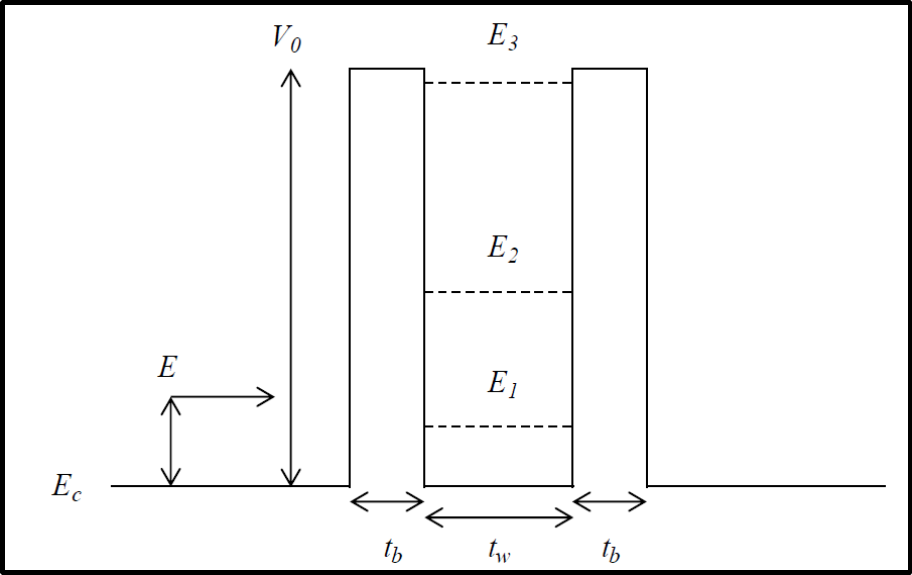
53
Figure 2.10. Schematic of quantum-well with finite barrier height structure. (where E is the incident
electron energy, EC is the conduction band, E1 and E2 are the first and second quantisation energies
respectively, V0 is the barrier height, tw and tb are the quantum-well thickness and the barrier
thickness respectively [57].
As a result of the decline in quantum-well thickness, the following implications occur:
1) Increases in the first resonant energy level increase the peak voltage required
to generate the peak current.
2) Nonetheless, the increase in the first resonant energy level has the beneficial
effect of lowering the barrier (
). As a result, the full-width at half-
maximum (FWHM) value will grow [78]. This approach to the Wentzel-
Kramers-Brillouin (WKB) approximation as described in equation (2.14). As a

54
result, as stated in equation (2.21), the transmission coefficient increases,
increasing the tunnelling current [59].
(2.21)
where
and
are the transmission coefficients of the left barrier and the right
barrier, respectively
3) The distance between adjacent resonant energy levels increases as the width of
the quantum well decreases. As a result of the reduction in leakage current
components at the second resonant energy level, the PVCR is projected to
increase.
2.5.3. Spacer thickness
Primary thinking behind the inclusion of the emitter and collector spacers is to reduce
dopant diffusion into the subsequent layer during growth; for example, dopant
diffusion from strongly doped n-InGaAs into the AlAs barrier. The band diagram of
an RTD with a spacer layer on both sides of the barriers under bias is shown in Figure
2.10. Due to an undoped or low-doped spacer layer between the emitter and the
barrier, and when a high applied voltage bias is applied, a triangular well forms at the
emitter barrier [54]. The confinement of this triangular well will generate a population
of 2D electron gas (2DEG) electrons in quasi-bound states. This population results in
resonant tunnelling between the quantised states in the triangle well and the resonant
state in the quantum well, a phenomenon referred to as 2D-2D resonant tunnelling.

55
As a result of the improved PVCR, a sharper resonance is noticed at a reduced current
density and often seen as a bump in the otherwise smooth I versus V characteristic
below resonance [54].
Figure 2.11. The band-diagram of RTD with the presence of the spacer layers on both sides of the
barriers [54].
State of the art in InGaAs/AlAs RTDs
THz radiation is most beneficial when it is generated from a coherent source and can
operate at room temperature. As a result, numerous studies have generated various
RTD architectures with varying oscillation frequencies and output powers. The best
candidate would be resonant tunnelling diodes due to their fast speed and small size.
In 1984, one of the earliest attempts to show an RTD experimentally occurred, and it
functioned at 18 GHz with a 5 μW output power [81]. The oscillation frequency was
56
increased numerous times until it reached several hundred GHz [59, 61]. In 1991, it
was claimed that an RTD with a fundamental oscillation of 712 GHz had been
developed [55]. A 64-element arrayed oscillator with RTDs was proposed with an
oscillation frequency of 650 GHz [82]. A harmonic oscillation frequency greater than
1 THz has been observed [83]. A fundamental oscillation of 650 GHz and a harmonic
oscillation of 1 THz were reported, while the output power at 1 THz was 60 μW [69].
The fundamental oscillation frequency climbed to 831 GHz in 2009 [84] and exceeded
1 THz in 2010 [85]. The fundamental oscillation frequency has been demonstrated by
numerous examples and exceeded 1.1 THz [19, 71, 86, 87]. The highest oscillation
frequency achieved is 1.98 THz, which was accomplished by increasing the antenna
electrode thickness to 2μm [17].
Summary
This chapter discussed quantum tunnelling theory and the development of the first
tunnelling diode using the Molecular Beam Epitaxy (MBE) technology and later
Metal-Organic Chemical Vapour Deposition (MOCVD). The essential operation of
Esaki's diode was then described. Since Esaki and Tsu established the concept of
resonant tunnelling in a finite double barrier structure, the double-barrier quantum-
well RTD structure has been the most often employed. The most useful RTD material
systems have been those using group IIIV compound semiconductors because of their
capacity to enhance electron mobility through band-gap engineering. The structure of
57
the epi-layers and the operating concept of the DBQW RTD have been described in
depth.
Additionally, this chapter discussed the DC and RF properties and how to extract or
compute them. Additionally, the implications of layer thickness on RTD performance
have been discussed. Finally, the state of the art has been discussed in the
InGaAs/AlAs RTD. The following chapter will examine the physical modelling of the
RTD's new structures.
58
3. CHAPTER 3: PHYSICAL MODELLING OF ASYMMETRICAL
SPACERS RESONANT TUNNELLING DIODES (RTDs)
3.1. Introduction
This chapter presents a detailed numerical investigation of asymmetrical spacers
resonant tunnelling diodes (RTDs). It optimises device performance by varying layer
thicknesses. This chapter also provides an overview of the relevant literature on
asymmetrical spacers resonant tunnelling diodes (RTDs). It is critical to validate the
physical model of formerly fabricated devices before proceeding with the
optimisation analysis of such a device. This chapter used the SILVACO ATLAS
software tool to conduct all physical modelling and analysis.
3.2. State of the art in Asymmetrical spacers RTDs
The oscillation frequency was the primary focus of previous research on RTDs. Thus,
various methods for increasing the oscillation frequency were proposed. One method
is to reduce the mesa area; however, this method may decrease the absolute value of
the negative differential conductance (NDC) and increase the series resistance [84].
Another technique for increasing the oscillation frequency is to decrease the RTD's
capacitance by thickening the collector spacer [88]. As Figure 3.1 below shows,
Professor Asada's group fabricated RTDs with varying collector spacer thicknesses.
They discovered that increasing the collector thickness increased the peak voltage and
voltage width ∆V of the NDR region. They also found that the current density is

59
independent of the collector spacer thickness as it is determined by the amount of
electron concentration in the emitter and the transmission coefficient of the double
barrier region.
Figure 3.1. The structure of the asymmetrical spacer RTD proposed by [88].
Figure 3.2. The oscillation frequency versus the spacer thickness with the I-V characteristics of
asymmetrical spacers RTDs [88].
60
They observed an increase in oscillation frequency from 325 GHz to 425 GHz when
the collector spacer thickness was increased from 5nm to 45nm, as illustrated in Figure
3.2 [86]. The oscillation frequency was increased to 831 GHz by decreasing the barrier
thickness from 1.5nm to 1.4nm and increasing the collector and emitter spacer
thicknesses to 20nm and 2nm, respectively [82]. Additionally, the peak and valley
voltage points increased as the collector spacer thickness increased. More oscillation
frequency improvement has been achieved by optimising the collector spacer
thickness alone [89] or the slot antenna length and thickness [17, 90]. While this
method increases the oscillation frequency by lowering the RTD capacitance, it also
increases the intrinsic delay time of the RTD by increasing the transit time in the
collector depletion region, making the RTD slower [91].
Additionally, increasing the collector spacer may increase the peak voltage point,
resulting in increased power dissipation. Consequently, the peak voltage point has to
be lowered, reducing power dissipation. Thus, by increasing the thickness of the
emitter spacer, the capacitance of the RTD can be reduced, increasing the oscillation
frequency without increasing the transit time across the collector depletion region
[90].
The authors of [92] investigated the effect of emitter spacer thickness on peak current
density using the numerical solution to the Schrödinger equation. They discovered
that an optimal emitter spacer thickness results in a high current density with a low
peak voltage. The collector spacer was 10nm thick. Two asymmetrical spacers RTDs

61
(mesa area= 3µm
2
and 5µm
2
) with the structure depicted in Figure 3.3 below have been
demonstrated theoretically and experimentally. The authors discovered that high
output power of 3.1 mW at 300 GHz and 1.8 mW at 600 GHz is possible [93].
Figure 3.3. The structure of asymmetrical spacers RTDs reported and studied in [93]
Additionally, the voltage span of the NDR region increases as the emitter spacer
thickness increases. There are only a few theoretical studies on RTDs with
asymmetrical spacers and thick emitter spacers. However, most of them focus
exclusively on the emitter spacer, omitting the collector spacer from the structure,
which is not the case with our devices.
62
3.3. Physical modelling of asymmetrical spacers RTDs Tunnelling Diodes by
SILVACO ATLAS tool
Due to the lengthy and expensive fabricating of semiconductor devices, it is frequently
faster and more cost-effective to explore new device concepts using physical
modelling and simulation. Physical modelling has been utilised extensively
throughout this research to assist and advise the development of new device
structures and to optimise device performance. This process has been simplified over
time using technology-computer-assisted design (TCAD) software such as SILVACO
ATLAS. This section will begin with a brief overview of the SILVACO ATLAS TCAD
software's features. This will include a discussion of how ATLAS defines devices as
part of the physical model. Additionally, this work discusses the utilised material
models, the incorporation of traps and defects, the physical simulation models, the
specification of doping levels, and the incorporation of contacts. The physical
modelling of RTDs will then be discussed.
3.3.1. SILVACO ATLAS
SILVACO is a simulator developed for the physical modelling and characterisation of
electronic devices. Numerous semiconductor fabrications and in-house designs have
benefited from the contribution of the SILVACO simulator to the development of the
"technology behind the chip". SILVACO expanded its simulator operation to include
analogue, mixed-signal, and RF circuit simulation and design as its presence in the
Electronic Design Automation (EDA) and Technology Computer-Aided Design

63
(TCAD) fields expanded. This simulator consists of a Virtual Wafer Fabrication (VWF)
simulator capable of simulating two-dimensional and three-dimensional physical
devices [94]. SILVACO allows users to model devices in a wide range of
environments, including electrical, thermal, and optical, under various bias
conditions. This robust simulator has the ability to generate precise and accurate
analysis of results, which is a significant advantage. ATLAS is a product from
SILVACO that is used to simulate devices. ATLAS is primarily composed of a
command file named Deckbuild, which refers to the location of the program's source
code. It includes syntax and commands for defining or modelling any specified
structure, material, or physical feature of electronic devices. ATLAS solves all
structures automatically by analysing log and structure files. TonyPlot is then used to
visualise both the statistical and model analyses. TonyPlot is a tool that visualises the
simulation output graphically. The SILVACO ATLAS flowchart is depicted in Figure
3.4.
Figure 3.4. SILVACO ATLAS inputs and outputs [94].
64
During the device simulation process, the device is defined in the device structure
command file, which contains the parameters and execution instructions of the device.
The simulator outcome consists of three distinct file types: 1) Runtime Output, which
shows the program's progress, error, and alerts to the user; 2) A Log File, which stores
all node voltage and current measurements from the device analysis; and 3) Solution
Files, which store 2D and 3D data relating to solution values at the applied bias point
across devices.
The 2D structure of the studied device is defined in DeckBuild using the ATLAS
syntax. The Region statement is used to define the structure in ATLAS Deckbuild,
isolating the selected location of the device. It accomplishes this by dividing the initial
mesh statement into different blocks. Afterwards, the Region number is used to set
the initial material parameters, which can be referred to later. The mesh should be
appointed to a region, with the region numbers arranged in ascending order. The
Region statement introduces the tunnel structure into the device modelling. This
assertion is contingent upon the solver used in the SILVACO modelling. The tunnel
structure region is defined as qtregion (i.e. quantum tunnelling region) in the
Semiconductor-Insulator-Semiconductor (SIS) solver. In contrast, the tunnel structure
region is defined using the Model statement in the Non-Equilibrium Green Function
(NEGF) solver.
Typically, the device structure is defined using 2D or 3D geometric grids. In spite of
this, the current tunnelling model implemented in SILVACO ATLAS emerged to be
65
quasi-one-dimensional and was therefore analysed on a sequence of parallel or
roughly parallel slices through the insulator. The type of mesh determines the
specifics of the implementation. Since the simulation employs a two-dimensional
structure, the mesh was defined in the x and y planes, with the x-plane denoting the
horizontal plane and the y-plane denoting the vertical plane. All coordinates were
given in microns. The spacing parameter was utilised to improve the accuracy and
precision of the analysis at a particular location. The mesh statement then created a
rectangular mesh on which all aspects of quantum tunnelling were computed. In
addition to Region and Mesh, the structure specification also includes a Doping
statement. This statement establishes the doping levels within the previously
designated regions. By default, the simulator simulates with silicon materials
parameters as a base material. The electrode command is the final command in the
structure specification that implements a comprehensive model structure. Based on
an electrically analysed device area, this statement is defined. In this study, anode and
cathode designations were assigned to all tunnel structure electrodes. The anode was
positioned at the high point of the epitaxial layer. Concurrently, the cathode is situated
directly above the device collector ohmic contact. Contact corresponds to the physical
property of an electrode. By default, an ohmic contact is assumed to exist between an
electrode and a semiconductor material. If a workfunction is defined, the electrode is
regarded as a Schottky contact. A Schottky Barrier (SB) contact's metal workfunction
was specified using the contact statement.
66
To improve the fitting of experimental data for materials with a high indium (In)
content, material parameters were determined. The materials used in physical
parameters were linked to the materials used in the mesh system. For standard
semiconductors such as silicon, GaAs, and AlAs, the parameters in ATLAS Deckbuild
were set to default values. As the database of material parameters gathered by our
group at the University of Manchester over the years became more accurate and
precise, the modelling for the lattice-matched system appeared quite progressive.
Typically, new materials require user-defined parameters, particularly for energy
bandgap, conduction and valence effective masses, and effective density of states at
300 K. In addition, it was essential to validate and precisely define each of the
necessary parameters in the section for material parameters [92].
The difference in bandgaps created an abrupt discontinuity in the valence and
conduction bands. At equilibrium, the energy band diagram of a modelled device
illustrates data on various parameters, such as barrier height, the width of the
quantum well formed between the two barriers, the degree of band bending in the
emitter and collector regions, and the spacer layers formed following the heavy
doping in the doped layer. The material parameters have the most significant
influence on the band diagram (i.e. electron affinities, energy bandgaps, effective
masses, and permittivity). As a result, the following sections present and discuss
additional details on physical device models and parameters that govern the model.
- Indium Gallium Arsenide (InGaAs) Material Parameters

67
Unlike the binary material GaAs, the tertiary material definition for InGaAs used the
Gallium composition fraction x in In(1-x)Ga(x)As. Due to the fact that the composition of
the compound semiconductors utilized in this structure differed from the ATLAS
configuration (In0.5Ga0.5As), the user was required to define a number of parameters.
Because of the unusual composition, the parameters were computed based on the
semiconductor parameter definition [93]. As a result, the effective electron mass,
dielectric constant, electron affinity, and bandgap energy of this ternary alloy were
defined using equations (3.1) to (3.4). Figure 3.5 shows these parameters for different
fractions such as In0.53Ga0.47As and GaAs.
Figure 3.5. The electron effective mass, Dielectric constant, and the Energy bandgap at 300K as a
function of the composition fraction (x)
(3.1)
68
(3.2)
(3.3)
(3.4)
- Aluminium Arsenide (AlAs) Material Parameters
The indirect bandgap of thick (or bulk) AlAs is typically 2.16 eV. However, when the
barrier thickness is 10 ML (28.3 Å), the - direct tunnelling with a 3.15 eV energy barrier
is dominant [95]. The -X current made a negligible contribution and thus was omitted
from the physical model. In terms of AlAs tunnelling effective mass (me,t), the Γ-valley
effective mass was lower than the X-valley effective mass due to the steeper curvature.
The effective mass of the electron, me*, was determined to be 0.15m0 in this work, in
accordance with [96].
The electron affinity of the barrier material is another critical parameter. The energy
difference between an electron's vacuum level and the bottom of the conduction band
edge is defined as its electron affinity [57]. This determines the band discontinuities at
semiconductor hetero-interfaces, specifically at the ΔEC and ΔEV interfaces. The
discontinuities in the conduction band (ΔEC) can be defined as follows:
(3.5)
The value of Δ for In0.53Ga0.47As/AlAs RTD was fixed at 1.69 eV in the command
file, consistent with the SILVACO ATLAS results shown in Figure 3.6. Thus, the

69
electron affinity of AlAs and In0.53Ga0.47As/AlAs were fixed at 2.91 eV and 4.6 eV,
respectively.
Figure 3.6. In0.53Ga0.47As/AlAs conduction band diagram profile at zero bias.
The Model statement specifies the model flags that indicate the inclusion of various
physical mechanisms, models, and other parameters in the simulation, such as global
temperature. To accurately model a specific phenomenon, the Model statement
parameters should be accurate, as flag setting requires differing mathematical models,
physical mechanisms, and other global parameters, such as substrate temperature.
Indeed, this simulator incorporates a variety of numerical methods for resolving
semiconductor device problems. The numerical method specification was
incorporated into the Method statements of the input file. The solution is defined in
the final section of this physical modelling. Obtaining solutions is comparable to
setting up a laboratory's parametric test equipment for device measurement. The user
-1
-0.5
0
0.5
1
1.5
2
0 0.02 0.04 0.06 0.08 0.1 0.12 0.14
Electron Energy (eV)
Thickness (μm)

70
must specify the voltages at each electrode. The simulation output is displayed in a
log and a solution file format. The user must first define the log and solve and save
the statement in the ATLAS simulation to run this file. Together, these statements offer
data for other functions to analyse. This study analysed the I-V characteristics, energy
band diagram, and other outputs of the device using three statements. Once the
simulator reached the solve statement, the problem-solution was enabled. Later, the
log statement was used to save any DC, transient, or AC data generated by the solve
statement. The saved statement assigned all data points in the output file to a node.
Before proceeding to the next section, the solvers associated with the model used in
this work, namely SIS and NEGF, are discussed.
- Non-Equilibrium Green Function (NEGF) Solver
The ATLAS model includes the charge associated with the quantisation effect in
strong quantum confinement. Thus, the NEGF solver would enable the Schrodinger-
Poisson solver to evaluate the tunnelling current, resulting in the current being
calculated as a sum over eigenstates. Using the following equation, the SILVACO
NEGF solver computed the current density through the barrier and quantum
confinement:
(3.6)
71
where , q, k, and denote the semiconductor's effective mass, electron charges,
Boltzmann constant, and the reduced Plank constant, respectively. Meanwhile, EFr and
EFl are the quasi-fermi levels on the barrier's right and left sides, respectively.
NEGF was used in the ATLAS simulator to determine carrier tunnelling in the
Negative Differential Region (NDR) through imposing quasi-equilibrium
requirements on the device's emitter and collector regions [97]. To incorporate this
model into the simulator, the user must define the NEGF modes in the model
statement using either N.NEGF PL or P.NEGF PL to activate planar NEGF solver for
electrons or for holes. The N.NEGF PL was used because the investigated structure
was based on the electrons.
Additionally, three conditions had to be met for this model to function correctly. First,
the device's quasi-equilibrium region was defined by defining Equil.NEGF on both
the emitter and collector sides. Following that, the ETA.NEGF parameter was
included in the model statement to set the broadening for characterising the Quasi-
equilibrium regions. Finally, Esize.NEGF was used to configure the NEGF solver's
energy grid points. In the case of insufficient convergence, the energy grid's size (i.e.
Esize.NEGF in the Model statement) and the magnitude of the broadening in quasi-
equilibrium regions were increased.
- Semiconductor-Insulator-Semiconductor, SIS Solver
The probability that an electron with energy E tunnels through the barrier was
determined by solving the Schrodinger equation using the transfer matrix method
72
(TMM) [94]. TMM [98-100] found the solution to the equation by discretizing the
device band profile and computing the transfer matrix, which contained potential
energy and effective mass. Regarding quantum mechanical tunnelling, because it is
treated as a wave, the tunnelling process can be assumed to be elastic. The current
density through the barrier was calculated using the equation 3.6 by SILVACO's SIS
solver.
The Non-local Quantum Barrier Tunnelling Model demonstrated SIS in SILVACO
ATLAS. Using SIS, the simulator calculated the tunnelling current between two
semiconductor regions separated by a potential barrier [101-103]. Previously, it was
assumed that the charge passed through the entire barrier with the source or sink at
the semiconductor regions' interface. To incorporate the model into the simulator, the
Model statement required the definition of "sis.el sis.ho" to enable direct electron
quantum tunneling through an insulator between two semiconductor regions.
Because the devices under investigation were doped with n-type carriers, SIS.EL was
used to simulate electron tunnelling. In the event of insufficient convergence, the
Model statement flag SIS.NLDERIVS was activated. This resulted in the incorporation
of non-local couplings into the system matrix. After creating the model, the user must
inform the simulator of the barrier structure's location. The most straightforward
technique is to specify the quantum tunnelling region by including the qtregion
parameter in each Region statement that defines a quantum barrier. It injects
tunnelling current at the interface's precise location and its lower carrier energy side.
73
The current after the NDR region, where thermal diffusion occurs, was calculated
using the SIS model.
3.3.2. Model Validation
Prior to designing a new structure for an RTD, it is necessary to validate that the
results of physical modelling are consistent with actual RTD measured results. Thus,
physical modelling and validation of fabricated RTD samples should be undertaken.
The RTD sample XMBE#300, fabricated at the University of Manchester [68], has a
mesa size of 1x2 μm
2
. Its epi-layer structure and material parameters are listed in Table
3.1. As illustrated in Table 3.1, XMBE#300 contains symmetrical spacers. Figure 3.6
illustrates the conduction band of the DBQW RTD sample XMBE#300 at zero bias, and
it is obvious that the emitter and collector regions are heavily doped. The conduction
band at the peak voltage is depicted in Figure 3.7. (0.177V).
The modelled and measured data for the XMBE#300 with a mesa size of 1x2 μm
2
are
shown in Figure 3.8. The peak current density of the simulated data was 1.2 mA/μm
2
at 0.175 V. In comparison, the measured data had a peak current density of 1.17
mA/μm
2
at 0.177 V. The simulated data had a valley current density of 0.191 mA/μm
2
at 0.295 V. In contrast, the measured data had a valley current density of 0.31 mA/μm
2
at 0.423 V. PVCR of simulated data was 6.3, which was greater than that of measured
data (i.e. 3.8). The I-V characteristics of the measured and modelled RTDs are shown
in Table 3.2.

74
Figure 3.7. The conduction band of the RTD sample XMBE#300 at peak voltage (0.177V).
Figure 3.8. The Physical modelling results of the RTD sample XMBE#300
The difference between the measured and simulated valley currents was due to the
software tool's inability to account for the parasitics of the measuring equipment. In
addition, the discrepancy between the modelled and measured values prior to the
peak voltage suggests that the formation of the 2D states in the emitter spacers may
-1
-0.5
0
0.5
1
1.5
2
0 0.02 0.04 0.06 0.08 0.1 0.12 0.14
Electron Energy (eV)
Thickness (μm)
0
0.5
1
1.5
2
2.5
3
0 0.1 0.2 0.3 0.4 0.5 0.6 0.7
Current (mA)
Voltage (V)
Measured data
Modelled data

75
not have been modelled accurately. Another explanation for the difference between
the modelled and measured data could be the self-heating of the device during
processing. Although there was a difference between the physical model and the
measurement of valley current and voltage, which affected the NDC, PVCR, and
maximum output power values, the physical model could be an excellent fit for circuit
design and investigation of other RTD structures.
Table 3.1. The epi-layers and material parameters of the XMBE#300 sample [68].
Layer
Material
Doping
(cm
-3
)
Thickness
(nm)
Bandgap (eV)
Ohmic layer
In0.53Ga0.47As(n++)
2E+19
45
0.75
Emitter
In0.53Ga0.47As(n+)
3E+18
25
0.75
Spacer
In0.53Ga0.47As
undoped
5
0.75
Barrier
AlAs
undoped
1.2
3.15 (direct)
Quantum Well
In0.8Ga0.2As
undoped
4.5
0.5
Barrier
AlAs
undoped
1.2
3.15 (direct)
Spacer
In0.53Ga0.47As
undoped
5
0.75
Collector
In0.53Ga0.47As(n+)
3E+18
25
0.75
Ohmic layer
In0.53Ga0.47As(n++)
1E+19
400
0.75
Substrate
InP

76
Table 3.2.The DC characteristics of the measured and modelled RTDs
I
P
(mA)
V
P
(V)
I
V
(mA)
V
V
(V)
|ΔI|
(mA)
|ΔV|
(V)
PVCR
|G
n
|
(mS)
P
max
(μW)
Measured
2.34
0.177
0.619
0.423
1.7
0.246
3.8
11
78
Modelled
2.41
0.175
0.381
0.295
2.03
0.12
6.3
25
46
3.4. Asymmetrical spacers RTDs with a fixed quantum-well thickness
After validating the physical model of sample XMBE#300, the same structure as in
Table 3.1 was used but with emitter and collector spacer thicknesses ranging from
1nm to 10nm to investigate the effects of asymmetrical spacers on the RTD's DC and
RF characteristics. Only the thickness of the emitter spacer was varied in [104], and
only in 2.5nm steps. Both spacers' thicknesses were varied in this study, with a 1nm
step. This step was performed in small steps to demonstrate clearly that increasing the
thickness of the emitter spacer decreases peak voltage while maintaining the
oscillation frequency and increasing the thickness of the collector spacer increases
peak voltage while decreasing the oscillation frequency.
3.4.1. DC characteristics
This section will demonstrate how the thickness of the emitter and collector spacer
affects RTD performance in terms of peak voltage, peak current, peak-to-valley
current ratio, negative differential conductance, and maximum dc output power.
- Peak Voltage (VP)
77
Increasing the thickness of the emitter spacer while maintaining a thin collector spacer
resulted in a low peak voltage. In contrast, RTDs with a thick collector spacer and a
thin emitter spacer had a high peak voltage. As illustrated in Figure 3.9, the peak
voltage of the RTDs with symmetric spacers would be in the moderate range. When
the collector spacer was thicker than the emitter spacer, it appeared that the peak
voltage was increasing, which would result in a significant increase in power
dissipation. This work aims to present RTDs suitable for low DC power consumption
applications; thus, increasing the peak voltage by thickening the collector spacer
would not aid in accomplishing this goal.
Additionally, the voltage span, defined as the difference between the peak and valley
voltages, increased with the thickness of the emitter and collector spacers, but at a
greater rate for thick emitter spacer RTDs than thick collector spacer RTDs. The
voltage span was maximum when both spacers were thick and symmetrical, as shown
in Figure 3.10. When the collector spacer was significantly thinner than the emitter
spacer (e.g. tcs=1nm, tes=10nm), the peak voltage was extremely low, which could result
in low NDC and DC output power. The RTD would not generate enough current to
operate in the NDR region in this case.

78
Figure 3.9. Effect of Emitter and Collector spacers on the peak voltage
Figure 3.10. The voltage span as the thickness of the collector and emitter spacers varies
- Peak Current (IP)

79
While thickening the emitter spacer resulted in a lower peak voltage, it also resulted
in a reduction in peak current due to the thickening of the triangular well formed
between the emitter region and the quantum well. As a result, electrons would have
more direct tunnelling into the quantum well than with the thin emitter spacer RTDs.
The Peak current was extremely high when the collector spacer was thicker than the
emitter spacer. However, this condition probably applied until the emitter spacer
thickness reached 3nm. When the thickness of the emitter spacer reached 3nm, the
peak current reached the moderate range, as shown in Figure 3.11. A significant peak
current resulted in increased power dissipation, conceptually similar to a high peak
voltage.
Figure 3.11. Effect of Emitter and Collector spacers on the peak current
- Peak-to-Valley Current ratio (PVCR)

80
The PVCR varies according to the peak and valley currents. Because the peak current
for thick collector spacer RTDs was high, the PVCR was very high, which could be
due to a decrease in the valley current. On the other hand, RTDs with emitter spacer
thicknesses greater than 2nm would maintain a moderate or slightly higher PVCR.
Such an RTD characteristic demonstrates how critical it is to maintain a moderate or
high PVCR when designing RF circuit amplifiers with microwatt DC power
consumption [105]. Figure 3.12 depicts the PVCR as the thickness of the emitter and
collector spacers changes.
Figure 3.12. Effect of Emitter and Collector spacers on the peak-to-valley current ratio
- Negative Differential Conductance (|Gn|)
NDC was determined by the difference between the peak and valley voltages and
currents; thus, a thick emitter spacer resulted in a low NDC, whereas a thick collector

81
spacer resulted in a high NDC. As illustrated in Figure 3.13, RTDs with symmetric
spacers of up to 3nm thickness exhibited a high NDC. However, symmetric spacer
RTDs with thicknesses of 8nm exhibited an extremely low NDC. As a result,
asymmetrical spacer RTDs with thicknesses ranging from 3 to 7nm would provide a
moderate NDC, allowing the RTD to operate with a low peak voltage and a moderate
peak current.
Figure 3.13. The NDC as the thickness of the collector and emitter spacers vary
- Maximum DC Output Power (PDC-MAX)
Similarly to NDC, the maximum dc output power (PDC-MAX) is determined by the
difference between the peak and valley voltages and currents, so a thick emitter spacer
resulted in a low PDC-MAX while including a thick collector spacer resulted in a high PDC-
MAX. As shown in Figure 3.14, RTDs with symmetric spacers with thicknesses up to

82
3nm had a high PDC-MAX. However, symmetric spacers RTDs with thicknesses of 8nm
had a very low PDC-MAX. As a result, asymmetrical spacer RTDs with thicknesses
ranging from 3nm to 7nm would have a moderate PDC-MAX, allowing the RTD to operate
while maintaining a low peak voltage and a moderate peak current.
Figure 3.14. The effect of varying the thickness of emitter and collector spacers on the Maximum DC
Output Power
RTDs with a thicker emitter spacer than a collector spacer (i.e. tcs=1nm, tes=10nm) had
a very low PDC-MAX, which is unsuitable for many RF applications. The NDC and PDC-
MAX could be improved using thin quantum wells. This improvement is attributed to
an increase in peak current, which will be discussed further in the following section.

83
3.4.2. RF Characteristics
The transport time (
) must be obtained before the RTD capacitance can be
calculated. This characteristic is required for determining whether RTD structures are
suitable for use as terahertz emitters. The transit time through the double barrier
quantum well was calculated using equation 2.12 from the previous chapter. The
transit time through the depletion region was calculated using equation 2.11 from the
previous chapter. To determine the transit time through the depletion region, the
thickness of the collector depletion region must be determined from the simulation
results, as illustrated in Figure 3.15.
Figure 3.15. Extraction of the thickness of the collector depletion region from the simulation results at
peak voltage (0.177V).
-1.5
-1
-0.5
0
0.5
1
1.5
0 0.02 0.04 0.06 0.08 0.1 0.12
Electron Energy (eV)
Thickness (μm)
d
collector depletion

84
Figure 3.16. The RTD transit time for RTDs with different thicknesses of emitter and collector spacers.
After calculating the RTD transit time and presenting it in Figure 3.16, the capacitance
of the RTD was determined and displayed in Figure 3.17. As illustrated in Figure 3.16
above, increasing the thickness of the emitter spacer seemed to have a minor impact
on the RTD transit time, whereas increasing the thickness of the collector spacer had
a significant effect. This increase was attributed to the increase in transit time through
the collector depletion region. Compared to the RTDs with thicker collector spacer
thicknesses, RTDs with collector spacer thicknesses up to 3nm would have a relatively
short transit time.
As illustrated in Figure 3.17 above, the decrease in RTD transit time have an impact
on decreasing RTD capacitance. When the emitter spacer was less than 3nm thick, and
the collector spacer was less than 5nm thick, the RTD capacitance was substantial

85
compared to thicker spacers. This was primarily due to the high capacitance of the
depletion region. Reduced RTD capacitance in thick emitter spacer RTDs would
support increased oscillation frequencies. The maximum operating frequency (fMAX)
was calculated using equation 2.16 from the previous chapter. Since the mesa area of
the devices was set to 1x2 μm
2
in this work, the series resistance of the RTD was
calculated to be 2.7 Ω using equation 2.10 from the previous chapter.
Figure 3.17. The effect of the emitter and collector spacers’ thicknesses on the RTD capacitance
As illustrated in Figure 3.18 below, changing the thickness of the emitter spacer did
not affect the maximum operation frequency, which was due to the short RTD transit
time and small RTD capacitance. On the other hand, due to the high NDC and small
RTD capacitance, very thick collector spacer RTDs would have a high maximum
operating frequency. Compared to other RTDs, RTDs with thin emitter and collector

86
spacers had larger NDC values, but this did not reflect into a higher maximum
operating frequency. The larger values of RTD capacitance prevented this.
Figure 3.18. The effect of the emitter and collector spacers’ thicknesses on the maximum operating
frequency
Despite the parasitic elements of the diodes that always limit high-frequency
operation, the intrinsic high-frequency limit due to both tunnelling and depletion
region delay times was given by equation 2.17 from the previous chapter. As
illustrated in Figure 3.19, increasing the thickness of the emitter spacer did not affect
the intrinsic limit frequency; however, increasing the thickness of the collector spacer
reduced the intrinsic limit frequency. This was because RTDs with a thick emitter
spacer had a short transit time, whereas RTDs with a thick collector spacer had a long
transit time. Nevertheless, RTDs with a collector spacer of 3nm had a high intrinsic
limit frequency due to their short transit time.

87
Figure 3.19. The intrinsic limit frequency as the emitter and collector spacers’ thicknesses vary
The maximum dc output power shown in Figure 3.14 was not practical because the
calculated actual RF power would be degraded due to the NDC being reduced and
the RTD transit time being increased. Equation 2.18 from the previous chapter has
been used to calculate the RF actual power for four RTDs: a very thick collector spacer,
a very thick emitter spacer, and symmetric spacers.
As illustrated in Figure 3.20, a thick emitter spacer had a negligible effect on the
oscillation frequency compared to a thick collector spacer. The increase in calculated
actual RF power resulting from the thick collector spacer was insignificant compared
to the decrease in calculated actual RF power as a result of the thick emitter spacer.

88
Figure 3.20. The actual output power as a function of the frequency for three different RTD structures
According to the previous analysis, RTDs with thick emitter spacers had a higher
operating frequency and a lower peak voltage than RTDs with thick collector spacers.
Since the depletion collector region did not expand, increasing the emitter spacer's
thickness did not affect carrier transit time. Low peak current in RTDs with thick
emitter spacers, on the other hand, resulted in low NDC and output power. RTDs with
a collector spacer of 3nm and an emitter spacer greater than 3nm demonstrated
excellent RF characteristics. As a result, the following two sections will discuss how to
modify RTDs with thick emitter spacers to increase peak current density and NDC
while maintaining a low peak voltage and high operating frequency.
1.E-06
1.E-05
1.E-04
0 200 400 600 800
Actual Output power (W)
Frequency (GHz)
tes=1nm, tcs=10nm
tes=10nm, tcs=1nm
tes=1nm, tcs=1nm
89
3.5. Asymmetrical spacers RTDs with varying quantum-well thickness
As previously stated, RTDs with thick emitter spacers required additional
modifications to increase the oscillation frequency while maintaining high NDC and
output power. As a result, one of the proposed modifications was to reduce the
quantum well's thickness. As mentioned in Section 2.5.2, decreasing the quantum well
thickness increases the current density, the NDC, and the maximum dc output power.
Several studies have found that decreasing the quantum well thickness increases the
oscillation frequency. Professor Asada's group reported that by reducing the quantum
well thickness of their asymmetrical spacers RTD from 4.5nm to 3.9nm and the barrier
thickness from 1.4nm to 1nm, they could increase the oscillation frequency to 1.31 THz
[19]. This increase was attributed to the carriers' transit time through the double
barriers quantum well (
) decreasing. By decreasing the quantum well thickness
from 3.9nm to 3nm, the oscillation frequency was increased to 1.42 THz with the help
of the reduced area and capacitance [106]. Further reduction in the quantum well
thickness (from 3nm to 2.5nm) resulted in an increase in the oscillation frequency to
1.92 THz [107].
All of these studies, however, used RTDs with thick collector spacers. Therefore, in
this section, RTDs with emitter spacers thicknesses ranging from 3nm to 10 nm were
investigated, with the quantum well thickness (tw) varying from 4.5nm to 2.5nm and
the emitter spacer thickness (tes) varying from 3nm to 10nm. As mentioned previously,
the collector spacer thickness (tcs) was 3nm because it demonstrated excellent RF

90
characteristics. Table 3.3 depicts the epi-layer structure of the investigated RTDs. The
DC and RF characteristics will be discussed in less detail than in the previous section
because the main topic of this section is the effect of varying the thickness of the
quantum well of the asymmetrical spacers RTDs.
Table 3.3. The epi-layers and material parameters of the proposed asymmetrical spacers RTDs with
varying the thicknesses of the emitter spacer and the quantum well
Layer
Material
Doping
(cm
-3
)
Thickness
(nm)
Bandgap (eV)
Ohmic layer
In0.53Ga0.47As(n++)
2E+19
45
0.75
Emitter
In0.53Ga0.47As(n+)
3E+18
25
0.75
Spacer
In0.53Ga0.47As
undoped
tes
0.75
Barrier
AlAs
undoped
1.2
3.15 (direct)
Quantum Well
In0.8Ga0.2As
undoped
tw
0.5
Barrier
AlAs
undoped
1.2
3.15 (direct)
Spacer
In0.53Ga0.47As
undoped
3
0.75
Collector
In0.53Ga0.47As(n+)
3E+18
25
0.75
Ohmic layer
In0.53Ga0.47As(n++)
1E+19
400
0.75
Substrate
InP

91
3.5.1. DC characteristics
The thick emitter spacer reduced the peak voltage of the RTDs with fixed quantum
well thickness. However, the peak voltage increased when the quantum well
thickness was reduced, as shown in Figure 3.21. This rise resulted from an increase in
the first resonant energy level. In terms of current density, RTDs with thin quantum
wells had higher current densities than RTDs with thicker quantum wells, as shown
in Figure 3.22. This increase was caused primarily by an increase in the transmission
coefficient.
Figure 3.21. The peak voltage (VP) of 1X2μm
2
asymmetrical spacers RTDs with varying the thickness
of the emitter spacer and the quantum well

92
Figure 3.22. The peak current (IP) as the thickness of the emitter spacer and the quantum well vary
Figure 3.23. Effect of varying the thickness of the Emitter spacer and the quantum well on the peak-to-
valley current ratio
93
RTDs with thick emitter spacers had lower current densities than RTDs with thin
emitter spacers. Due to the decrease in the separation between adjacent resonant
energy levels, the leakage current components through the second resonant energy
level would decrease. Thus, the PVCR would decrease, as shown in Figure 3.23.
Because current densities are lowered, the PVCR of RTDs with thick emitter spacers
and thick quantum wells was the lowest. The NDC and maximum dc output power
increased as current densities increased, as illustrated in Figures 3.24 and 3.25. Even
with thick emitter spacers, thin quantum well RTDs could achieve a high NDC and
output power. Due to their high NDC and output power, RTDs with thin quantum
wells are excellent for terahertz emitters in high-frequency applications.
Figure 3.24. The effect of varying the thickness of the emitter spacer and quantum well on the NDC
with 1X2μm
2
RTD mesa area.

94
Figure 3.25. The effect of varying the thickness of the emitter spacer and quantum well on the
Maximum DC Output Power with 1X2μm
2
RTD mesa area.
3.5.2. RF Characteristics
As mentioned previously, because the series resistance was fixed in this work (as the
mesa area was fixed), the oscillation frequency depends only on the RTD capacitance
and the NDC. The capacitance of the RTD is affected by the transit time and the
capacitance of the depletion layer. As illustrated in Figure 3.26, the transit time
decreased due to the reduced transit time through the double barrier quantum well
region and the collector depletion region.
Despite the decrease in transit time, the capacitance of the RTD increased as the
quantum well thickness decreased, as illustrated in Figure 3.27. This increase resulted
from the depletion region capacitance and quantum capacitance increasing. Quantum
capacitance increased due to the high NDC.

95
Figure 3.26. The change in the RTD transit time as the thickness of the emitter spacer and the
quantum well change
Figure 3.27. The effect of thinning the quantum well and thickening the emitter spacer on the RTD
capacitance

96
The RTDs with a thin quantum well of 2.5nm and a 10nm emitter spacer may have a
small RTD capacitance and a moderately short transit time, allowing these RTDs to
operate at the highest possible operating frequency, as illustrated in Figure 3.28. While
the thin quantum RTDs with a thin emitter spacer thickness was expected to have the
highest maximum operating frequency due to their high NDC, their operating
frequency was degraded due to their high RTD capacitance values. It appears as
though using a very thick emitter spacer thickness improved their operating
frequencies for all quantum well thicknesses, as illustrated in Figure 3.28.
Figure 3.28. The effect of varying the thickness of the quantum well and the emitter spacer on the
maximum operating frequency

97
Figure 3.29. The effect of thinning the quantum well and thickening the emitter spacer on the intrinsic
frequency limit
Figure 3.29 above depicts the effects of varying the thickness of the emitter and
collector spacer on the intrinsic frequency limit.
Due to the excellent performance of all quantum well thicknesses when combined
with a very thick emitter spacer (i.e. 10nm), their calculated actual RF power was
calculated to demonstrate their capability to provide high RF output power at high
frequency. The very thin quantum well RTDs (i.e. tw=2.5nm) had the highest
frequency. They could potentially deliver 1mW at frequencies as high as 630 GHz, as
illustrated in Figure 3.30. The RTDs with thick quantum wells (tw=4.5nm) had the
lowest output power and operating frequency.

98
Figure 3.30. The actual output power as a function of the frequency for thin quantum well RTDs with
very thick emitter spacers and 1X2μm
2
RTD mesa area
Even though the thin quantum wells had a high NDC, a high maximum dc output
power, and a high PVCR, their peak voltage and current increased, resulting in
increased power dissipation. Additionally, the RTD transit time decreased when
using a thinner quantum well. However, the RTD capacitance increased due to an
increase in the depletion region and quantum well capacitances. These findings
affected the maximum operating frequency of RTDs with thin quantum wells and
emitter spacers. In terms of other RF characteristics, decreasing the quantum well's
thickness increased the intrinsic limit frequency and calculated actual RF power.
According to the analysis in this section, the thin quantum well RTDs had excellent
DC and RF characteristics when the emitter spacer was as thick as 10nm. However,
4.E-06
4.E-05
4.E-04
4.E-03
0 200 400 600 800 1000
Actual Output power (W)
Frequency (GHz)
tcs=3nm, tes=10nm, tw=2.5nm tcs=3nm, tes=10nm, tw=3.5nm
tcs=3nm, tes=10nm, tw=4.5nm
99
the peak voltage must be reduced further to make it suitable for low-power
applications. The following section will discuss another modification to the RTD
structure that will further reduce the peak voltage.
3.6. Asymmetrical spacers RTDs with deep and thin quantum-wells
While RTDs with thin quantum wells and a thick emitter spacer could have a higher
NDC and output power, their peak voltage and current are also high, resulting in
increased power dissipation. Additionally, a higher peak voltage may reduce the
efficiency of the RTD by creating a strong electric field in the collector spacer layer. As
a result, additional modifications to asymmetrical spacer RTDs should be proposed to
decrease the peak voltage and increase RTD efficiency. Kanaya et al. hypothesised that
a deep well filled with indium-rich InGaAs could reduce the peak voltage due to the
quantum well bottom's depression [108]. The layer structure and band diagram of the
asymmetrical spacers RTDs proposed in [108] are depicted in Figure 3.30.
As illustrated in Figure 3.31, the emitter spacer is thicker (25nm) than the collector
spacer (i.e. 2nm). The oscillation frequency of the asymmetrical spacer RTD with a
deep and thin quantum well was 1.27 THz, while the asymmetrical spacer RTD
without a deep and narrow quantum well oscillated at 0.96 THz. The oscillation
frequency increase was attributed to the short dwell time and low RTD capacitance.
This section will investigate RTDs with a 3nm collector spacer and a 10nm emitter
spacer with deep and thin quantum wells. The Indium (In) composition in the InGaAs
quantum well varied between 0.8 and 0.95, and the quantum well thickness varied

100
between 4.5nm and 2.5nm. Table 3.4 illustrates the epi-layers structure of the modified
asymmetrical spacers RTD.
Figure 3.31. The epi-layer structure and the band diagram of the asymmetrical spacers RTD with deep
and thin quantum well reported in [108].
Since some of the DC and RF characteristics, such as NDC, maximum dc output
power, and intrinsic limit frequency, were improved by using thin quantum wells,
this section will focus exclusively on the DC and RF characteristics that required
improvements, such as peak voltage and current, transit time, RTD capacitance, and
maximum operating frequency.

101
Table 3.4. The epi-layers and material parameters of the modified asymmetrical spacers RTDs with
varying the thicknesses of the emitter spacer and Indium composition (x) in the quantum well
Layer
Material
Doping
(cm
-3
)
Thickness
(nm)
Bandgap (eV)
Ohmic layer
In0.53Ga0.47As(n++)
2E+19
45
0.75
Emitter
In0.53Ga0.47As(n+)
3E+18
25
0.75
Spacer
In0.53Ga0.47As
undoped
10
0.75
Barrier
AlAs
undoped
1.2
3.15 (direct)
Quantum Well
InXGa1-X2As
undoped
tw
Eg(x)
Barrier
AlAs
undoped
1.2
3.15 (direct)
Spacer
In0.53Ga0.47As
undoped
3
0.75
Collector
In0.53Ga0.47As(n+)
3E+18
25
0.75
Ohmic layer
In0.53Ga0.47As(n++)
1E+19
400
0.75
Substrate
InP

102
Figure 3.32. The effect of increasing the Indium composition in the quantum well on the peak voltage
of RTDs with various quantum well thicknesses
Figure 3.33. The peak current of asymmetrical spacers RTDs as the quantum well thickness and the
Indium composition vary
103
As shown in Figure 3.32 above, increasing the indium content in the quantum well
decreased the peak voltage point due to the material's narrow bandgap. For instance,
when the Indium composition was increased from 0.8 to 0.95, the peak voltage of
RTDs with a 2.5nm quantum well decreased from 0.83 V to 0.39 V. Additionally, RTDs
with quantum wells larger than 3.5nm had peak voltages less than 0.2 V, making them
suitable for ultra-low power consumption applications.
As with the peak voltage, the peak current has been reduced as the indium
composition has increased, as illustrated in Figure 3.33.
When the Indium composition was 0.95, only the RTDs with a 2.5nm quantum well
had a peak current greater than 10mA. In contrast, the other RTDs had much lower
peak currents. Peak current decreased rapidly for the same quantum well thickness;
for example, when the Indium composition was increased from 0.8 to 0.95, the peak
current of RTDs with a 2.5nm quantum well decreased from 37mA to 15mA. Because
the peak current decreased, it was expected that the PVCR would decrease as well.
Appendix B includes a figure illustrating the effect of increasing the Indium content
on the PVCR, as the PVCR is not the subject of this section.
As shown in Figure 3.34, the RTD transit time decreased as the Indium composition
increased, owing to the decrease in dwell time. For example, when the Indium
composition was increased from 0.8 to 0.95, the RTD transit time decreased from 283
fs to 237 fs.

104
Figure 3.34. The change in the RTD transit time as the thickness of the quantum well and the Indium
composition change
As illustrated in Figure 3.34, this decrease in the RTD transit time decreased the RTD
capacitance values. For example, when the Indium composition was increased from
0.8 to 0.95, the capacitance of RTDs with a 2.5nm quantum well decreased from 30 fF
to 19 fF. The decrease in RTD capacitance was caused by a decrease in both the RTD
transit time and the quantum capacitance. The decrease in quantum capacitance was
anticipated as the NDC decreased with increasing Indium composition. The NDC
decreased primarily as a result of low peak currents. Appendix B contains a graph
illustrating the effect of increasing the Indium content on the NDC.

105
Figure 3.35. The RTD capacitance of asymmetrical spacers RTDs as the quantum well thickness and
the Indium composition vary
As illustrated in Figure 3.35, the decrease in the RTD capacitance and the NDC
decreased the maximum operating frequency. This decrease could be avoided by
using quantum wells that are thinner and deeper. For example, RTDs with a 3.5nm
and 0.85 Indium composition had a maximum operating frequency of 591 GHz, which
was reduced to 530 GHz when the Indium composition was increased to 0.95;
however, using a thinner quantum well with a higher Indium concentration (i.e.
tw=3nm and x=0.9) increased the operating frequency to 630 GHz. Inevitably, as
transit times decreased, the intrinsic limit frequency increased. Appendix B includes
a figure demonstrating the effect of increasing the Indium content in the quantum well
on the intrinsic limit frequency.

106
Figure 3.36. The effect of varying the thickness of the quantum well and the Indium composition on
the maximum operating frequency
In terms of calculated actual RF power, increasing the Indium content reduced
calculated actual RF power. However, it increased oscillation frequency, as illustrated
in Figure 3.36. For example, when the Indium composition was increased from 0.8 to
0.85 and the oscillation frequency was increased from 774 to 791 GHz, the calculated
actual RF power of the RTDs with a 4nm quantum well decreased from 82 μW to 30
μW. As discussed previously, decreasing the quantum well thickness increased the
oscillation frequency and calculated actual RF power, as illustrated in Figure 3.36
when the quantum well thickness was reduced from 4nm to 3.5nm with a fixed
indium composition of 0.85. To increase the RF actual and oscillation frequency, the
Indium content should be increased, and the quantum well thickness should be
reduced. For instance, when the quantum well thickness was reduced from 3 to 2.5nm

107
and the Indium composition was increased from 0.9 to 0.95, the oscillation frequency
increased from 900 to 1055 GHz, and the calculated actual RF power increased from
312 to 963 μW.
Figure 3.37. The calculated actual RF power of RTDs with different quantum well thicknesses and
different Indium compositions
After discussing performance optimization for asymmetrical RTDs, this analysis
designed and examined RTD structures that exhibit excellent DC and RF
characteristics for various applications. Asymmetrical spacer RTDs with a 2.5nm
quantum well and a 0.95 Indium composition could produce 0.5 mW at a high
frequency of 690 GHz. These RTDs had a low peak voltage and a moderate peak
current while operating at frequencies greater than 1 THz. They also had a small RTD
capacitance and a significantly shorter RTD transit time. Not only high output power
1.E-06
1.E-05
1.E-04
1.E-03
1.E-02
0 200 400 600 800 1000 1200
Output power (W)
Frequency (GHz)
tw=2.5nm, x=0.95 tw=3nm, x=0.9 tw=3.5nm, x=0.85
tw=4nm, x=0.85 tw=4nm, x=0.8
108
RTDs, which are excellent candidates for use as THz emitters, but also RTDs with
relatively low peak voltages and currents while maintaining a high PVCR have been
designed, making them suitable for ultra-low power consumption applications.
3.7. Summary
This chapter began by summarising the pertinent literature on asymmetrical spacers
RTDs. Then, the SILVACO ATLAS simulation tool was discussed, which was used in
this chapter. Additionally, the two models utilised in this chapter were discussed. The
physical model was then validated using experimental data. The slight difference
between the simulated and measured data was caused by the simulation tool's
inability to simulate the measurement equipment’s parasitic effects and by the
inaccurate modelling of the formation of the 2D states in the emitter spacers. Another
explanation for the difference between the modelled and measured data could be the
self-heating of the device during processing. To demonstrate that increasing the
collector spacer thickness increases the peak voltage, thereby increasing power
dissipation, while decreasing the emitter spacer thickness decreases the peak voltage,
the thickness of the two spacers was varied between 1nm and 10nm. Although the
thick emitter spacer RTDs had low peak voltages, a large PVCR, a higher oscillation
frequency, a short RTD transit time, and a small RTD capacitance, their NDC and
output power were reduced.
Thus, to increase the NDC and output power, the quantum well thickness varied
between 4.5nm and 2.5nm. The emitter spacer thickness varied between 3nm and
109
10nm. The collector spacer thickness was maintained at 3nm. Although thin quantum
well RTDs had a high NDC, a large PVCR, a high output power, and a shorter RTD
transit time, they had a lower operating frequency, a larger RTD capacitance, and a
high peak voltage and current. The RTD structure was further modified by increasing
the amount of Indium in the quantum well. This modification decreases the peak
voltage and current and the oscillation frequency, the RTD transit time, and the RTD
capacitance. This chapter discussed RTDs suitable for high output power radio
frequency (RF) applications and RTDs suitable for low power or ultra-low power
radio frequency (RF) applications. Finally, this chapter's objective was to introduce
asymmetrical spacer RTDs and optimise their performance for various applications.
The following chapter will demonstrate the RTDs' performance in low-power
applications.
110
4. CHAPTER 4: DESIGN AND ANALYSIS OF 10 GHz RTD
BASED AMPLIFIER FOR WIRELESS COMMUNICATIONS
4.1. Introduction
In previous chapters, a thorough review of the literature and physical modelling of
resonant tunnelling diodes was conducted to establish the suitability and utility of the
tunnelling devices for microwave and THz applications. As a result, chapter four
focuses on the design and performance analysis of a narrow-band amplifier for
wireless communication systems that use resonant tunnelling diodes (RTDs). This
includes the design of passive components such as capacitors and spiral inductors and
their modelling. Additionally, this chapter summarises the pertinent literature
regarding RTDs as power amplifiers. It is critical to understand the fundamental
operation of reflection-based RTD power amplifiers before designing and analysing
such a device. The study's primary outcome is the realisation of a low-power DC
amplifier operating at 10 GHz. All design and analysis in this chapter were carried out
using the Advanced Design System (ADS) software tool.
4.2. Power amplifications using the resonant tunnelling diodes (RTDs)
Due to the RTD's unique negative differential conductance (NDC), transmission line
losses can be compensated for and used to provide gain. An RTD amplifier can be
realised in two circuit topologies: active transmission line amplifier or reflection-based
amplifier. The first attempt to use tunnel devices in conjunction with Field-Effect
111
Transistor (FET) amplification was made in 2003 [109]. The dc power output was
400μW with less than 5 dB gain. A group of researchers developed several RTD
amplifiers with high gain and excellent RF performance at frequencies around 5 GHz
[110-114]. Professor Missous and his group presented a modelling and theoretical
analysis of a high gain InGaAs/AlAs RTD reflection-based amplifier operating in the
K band in 2017 [115]. The amplifier achieved a gain of 32 dB with a very low DC power
consumption of 100 μW.
Due to the losses of the transmission lines (TLs), the RF signals propagating through
the active transmission line amplifier undergo a phase shift. As a result, we use
reflection-based amplifiers because they significantly reduce noise performance and
chip size.
The design steps for the RTD amplifier are comparable to those presented in [46, 115];
however, the main circuit was modified in this research to be consistent with the
amplifier circuit described in the literature. In addition, the operating frequency and
RTD sample are clearly different. Furthermore, this work presents the layout design
of the RTD amplifier and compares the results of the schematic simulation to the
layout design results, whereas [46, 115] only presented schematic results.
4.3. Principle operation of reflection-based RTD amplifier
In the reflection-based amplifier, the RF signal is reflected at appropriately terminated
ports to maintain a high gain at the output terminal. The RTD amplifier, as depicted
in Figure 4.1, comprises a single branch coupler and two similar RTDs. It is crucial to

112
explain the essential operation and critical factors of the branch coupler. First, the
signal is fed into the input port, and then it is split into two ports that are 90
0
degrees
out of phase. The signal is then reflected by the bypass capacitor CbP due to the
amplified signal (due to the NDR).
Figure 4.1. Schematic circuit of the RTD reflection-based amplifier model
The RTD port signals can then be merged in phase at the output port with a phase
difference of 270
0
degrees relative to the input signal at the input port. Furthermore,
because the reflected amplified signals are 180
0
degrees out of phase at the input port,
they cancel one another out [116]. To eliminate parasitic oscillations at low
frequencies, a bypass capacitance serves as a short circuit at undesirable frequencies
[114]. The magnitude of the reflection coefficient between the coupler and the RTDs is
used to define the amplifier's voltage gain as follows:
(4.1)
113
Because the two RTDs are charged at the coupler termination and operated in their
NDR region, the reflection in equation (4.1) will be greater than one. To mitigate
mismatching losses, the values of these impedances must be nearly identical. The
reflection-based amplifier is used because there is no requirement for a large matching
circuit. This is primarily because the output impedance of a single coupler depends
on the component values. As a result, the components of the single coupler can be
tuned to match the RTD's impedance (ZRTD). A coupler based on lumped elements has
been developed for MMIC application [117]. Before designing the RTD amplifier
circuit, it is necessary to discuss the software tool used in this chapter, ADS. The
following section will provide a brief overview of this software tool.
4.4. Advanced Design System (ADS) software tool
Advanced Design System (ADS) is the most comprehensive and user-friendly
electronic design automation tool available for high-frequency and high-speed
products [118]. Keysight Technologies boasts the industry's broadest support, with
over one hundred foundry processes supported by ADS. Additionally, it is the
primary design tool used by all major integrated circuit suppliers. The following are
brief descriptions of the two types of analysis performed by ADS in this chapter:
a. S-parameter simulation
Using the Simulation S-Param palette's S-parameter simulation controller (S-
Parameters), you can:
114
- Obtain the scattering parameters (S-parameters) of a component, circuit, or
subnetwork and convert them to Y- or Z-parameters.
- Plot the variations in swept-frequency S-parameters with another changing variable.
- Create simulations of group delay or linear noise.
- Simulate the effects of frequency conversion on the S-parameters of a mixer-based
circuit. (This is also referred to as frequency-translating network analysis.)
Additionally, the Simulation-S Param palette contains components for general
simulation and sweep options and a variety of measurement components for
calculating pertinent measurements.
b. Harmonic balance simulation (HB)
Harmonic balance is a high-precision frequency-domain analysis technique used to
determine the steady-state solution of nonlinear circuits and systems. It is frequently
used to simulate analogue RF and microwave problems in the frequency domain.
After calculating the steady-state solution, the harmonic balance simulator can be
used to perform the following tasks:
- Calculate third-order intercept (TOI) points, total harmonic distortion (THD), and
intermodulation distortion components.
- Analyse the load-pull contours of power amplifiers.
- Analyse nonlinear noise.
115
The harmonic balance method assumes that the input stimulus is composed of a small
number of steady-state sinusoids. As a result, the solution is a sum of steady-state
sinusoids that includes both the input and any significant harmonics or mixing terms.
ADS electromagnetic (EM) simulation is a 2.5D model based on a 2D component
layout that can display a three-dimensional viewpoint of radio frequency current flow
in transmission lines and far-field radiation patterns. Additionally, the EM simulation
tool can account for transmission line coupling. This results in a module that is more
accurate and can be easily expanded to anticipate the performance of the circuit even
before to fabrication and actual results [118]. Indeed, the EM model includes two main
simulators: momentum RF and momentum microwave, which were used in this
study. This is because of the fact that this mode employs full-wave Green's functions,
which are frequency-dependent and account for ground plane losses in the prime
elements resulting from high-frequency operation. Following these steps, momentum
was established. Due to the fact that the simulator divides transmission lines into
small cells during the simulation process, the mesh with the highest simulation
frequency was chosen. This insures that the mesh density of cells per wavelength is
sufficient, which leads to improved simulation performance. The sole disadvantage of
a high density mesh is that the simulation process takes longer to execute. The
conductor, dielectric, and lossy layers' electrical and physical parameters, such as
dimensions, conductivity, and relative permittivity, were defined in the simulator. For
the configuration of coplanar waveguides, a finite substrate thickness was used. The

116
model is evaluated without a ground plane at the back of the structure. This eliminates
effectively the parasitics associated with grounded coplanar structures (GCPW). This
simulation used a 625 μm thick semi-insulating InP substrate with a
of 12.5 and a
loss tangent () as low as 0.002 [119].
4.5. Modelling of Single branch coupler
A branch coupler comprises four microstrip lines, two of which have identical
impedance as the input and output ports. The other two ports' impedance is typically
expressed as
[120, 121]. Two critical parameters should be considered when
describing a branch coupler: the coupling factor (CF) and the directivity (Dcoupler),
which are specified in [122]:
(4.2)
(4.3)
where P1, P2, and P3 are denoted as the input power to port 1 and the output power
from ports 2 and 3, respectively.
To ensure an even power distribution between ports 3 and 4, the coupling factor (CF)
must be set to 3 dB. Couplers suitable for this application typically have a directivity
of 30-35 dB, which is critical to ensuring that the output power at port 2 is small
compared to the output power at port 3 [122]. An ADS model was created using ideal
transmission lines at a 10 GHz operating frequency to investigate the coupler
response, as illustrated in Figure 4.2.

117
Figure 4.2. The model of a single branch coupler with ideal transmission lines
Figure 4.3. The result of S-parameter simulation for single branch coupler modelled in ADS using
ideal transmission lines at 10 GHz
Because each term must produce a π/2 phase shift for the coupler to operate properly,
the electrical length was set to 90
0
. The simulation results indicate that the input power
-80
-60
-40
-20
0
5 6 7 8 9 10 11 12 13 14 15
S-Parameter Response (dB)
Frequency (GHz)
S(1,1) S(2,1)
S(3,1) S(4,1)

118
is evenly distributed between ports 3 and 4. A centre frequency of 10 GHz provides a
large 10dB bandwidth (i.e. 3.3 GHz), as illustrated in Figure 4.3. The reflection
performance at port 1 (S11 =-76.4 dB) and the received power at port 2 (S21 =-76.4 dB)
are excellent, as they are significantly less than -10 dB. In practice, such values are
difficult to achieve due to the effect of losses and parasitic, which are ignored at this
stage.
The single branch coupler was modelled using LC passive elements to model the
single branch coupler in its practical configuration, as illustrated in Figure 4.4 below.
Figure 4.4. The LC model of single branch coupler operating at 10 GHz using ADS software
These elements must be carefully adjusted to achieve a coupling factor of
approximately 3 dB and a directivity greater than 30 dB. As Figure 4.5 shows, the
coupler's performance is relatively similar to that of the first coupler with ideal
transmission lines.

119
Figure 4.5. The result of S-parameter simulation for single branch coupler modelled in ADS using LC
components at 10 GHz
The coupling factor and directivity can be determined as follows from the results of
S-parameter responses:
(4.4)
(4.5)
At operating frequency (i.e. 10 GHz), the coupling factor and directivity were
calculated to be 3 dB and 63.5 dB, respectively, contributing to the coupler's circuit's
excellent performance. Both S11 and S21 exhibit responses significantly less than -10 dB,
and the branch coupler exhibits a 3 dB power split. The mathematical formula for the
values of the LC elements in Figure 4.4 is:
(4.6)
-80
-60
-40
-20
0
5 6 7 8 9 10 11 12 13 14 15
S-Parameter Response (dB)
Frequency (GHz)
S(1,1) S(2,1)
S(3,1) S(4,1)

120
(4.7)
(4.8)
These equations hold only if all ports have a resistance of 50Ω. The values of the
lumped elements are shown in Table 4.1, and they are quite small.
Table 4.1. Values of LC elements in the LC single branch coupler
Component
Value
CS1
450 fF
CS2
450 fF
CP1
318 fF
CP2
318 fF
L1
330 pH
L2
330 pH
L3
330 pH
L4
330 pH
Coupler dimensions should be scaled down as the frequency increases due to the
decrease in the values of the LC elements. The LC single coupler is preferred up to a
specific frequency because the unavoidable parasitics are much smaller than the actual
circuit elements. Beyond this frequency, another design, such as a directional coupler
based on a co-planar waveguide, would be required. Otherwise, a multilayer MMIC
121
coupler may be required as proposed for wide-band amplifiers up to 60 GHz [121].
The next step is to design the amplifier circuit, including the single coupler and the
RTD, and evaluate the RTD amplifier's ability to provide the required gain and
functionality.
4.6. Simulation of RTD amplifier
This section discusses modelling a 10 GHz reflection-based amplifier using
InGaAs/AlAs NDR RTDs. The RTD sample XMBE#300, whose epi-layers structure
shows in Table 3.1, with a mesa area of 4x4 μm
2
, was chosen due to its low current
density (i.e. 1.17 mA/µm
2
). The large mesa area device was used to ensure that large
devices can also achieve a high gain at the output port while consuming little DC
power. This section discusses the extraction of the RTD resistance and capacitance.
Additionally, the passive components in the RTD amplifier circuit are modelled. The
final part will compare the results of the RTD amplifier's schematic and layout design.
4.6.1. Extraction of the RRTD and CRTD
Due to the absence of a representation block for the RTD in the ADS software tool, the
equivalent circuit for the RTD, as illustrated in Figure 4.6, should be used for circuit
analysis.

122
Figure 4.6. The equivalent circuit of the intrinsic RTD
Due to the difficulty of extracting equivalent circuit components from large area
device measurements in the NDR region, as stated in [46], the measured I-V
characteristics are fitted with a 3
rd
degree polynomial function to obtain the RRTD
illustrated in Figure 4.7 below. The excellent agreement between the measured and
fitted data is illustrated in Figure 4.7. The modelled RRTD is calculated using the
relationship
, as illustrated in Figure 4.7. To calculate the RTD
capacitance, the pre-peak and pre-valley measured points are used to calculate the
CRTD in the NDR region, as illustrated in Figure 4.8. When the bias voltage is 0.35 V,
the extracted RRTD is -100Ω, and the extracted CRTD is 100 fF. The calculated series
resistance is 0.5Ω.

123
Figure 4.7. Measured and fitted forward I-V characteristics as well as extracted junction resistance of
the RTD XMBE#300 with a 16μm
2
mesa size
Figure 4.8. Extraction of the RTD capacitance from the measured S-parameters
-100
-80
-60
-40
-20
0
20
40
60
80
100
0
5
10
15
20
25
30
0 0.05 0.1 0.15 0.2 0.25 0.3 0.35 0.4 0.45 0.5
Junction Resistance (
Ω)
Current (mA)
Voltage (V)
Measured data
Fitted data (Polynomial function)
Rj
40
60
80
100
120
140
160
180
0.1 0.15 0.2 0.25 0.3 0.35 0.4
Capacitance (fF)
Voltage (V)

124
The intrinsic device's actual S11 value lies outside the normalized Smith chart's unit
circle (|S11 > 1|), or it is greater than 0dB on the x-y graph, indicating that the reflected
power is greater than the incident power, as illustrated in Figure 4.9.
Figure 4.9. Left and right sides: measured S11 for intrinsic device sample #300 with a mesa area of
4×4μm2 biased in the NDR region plotted in smith chart and x-y graph, respectively.
This is because the RTD has a negative resistance, indicating that it can generate power
at the measured frequencies.
Because the input impedance of the RTD sample XMBE#300 (RRTD=-100Ω) is different
from the standard 50Ω, the LC components of the single coupler had to be carefully
optimised. For effective operation of the RTD amplifier circuit, the single branch
coupler's inductance should be between 510 and 610pH, and its capacitance should be
between 80 and 261fF.
To characterise the performance of the typical lumped-element hybrid coupler, which
consists of four spiral inductors and four MIM capacitors, a resistance of 100Ω and a

125
capacitance of 100fF were used in place of the RTDs on ports 3 and 4. S-parameters for
the designed coupler are depicted in Figure 4.10.
Figure 4.10. The result of S-parameter simulation for single branch coupler modelled in ADS using LC
components with a resistance of 100Ω and a capacitance of 100fF at 10 GHz
At the design frequency of 10 GHz, the coupler had return losses (S11) and isolations
(S21) of -44dB and -14.75dB. Transmission (S41) and coupling (S31) were simulated at -
4.53dB and -2.2dB, respectively.
4.6.2. Schematic circuit of the RTD amplifier
Before modelling the RTD amplifiers' passive components, a schematic circuit similar
to that shown in Figure 4.1 was designed using a single coupler and the RTD's
equivalent circuit. This procedure was performed to ensure that the RTD amplifier
could operate at 10 GHz. The RTD amplifier's schematic circuit is shown in Figure
4.11, and the LC components used in this circuit are listed in Table 4.2. Figure 4.12
-50
-40
-30
-20
-10
0
5 6 7 8 9 10 11 12 13 14 15
S-Parameter Response (dB)
Frequency (GHz)
S(1,1) S(2,1)
S(3,1) S(4,1)

126
illustrates the gain and S11 values obtained from the schematic circuit. At a frequency
of 10 GHz, the gain was 14.6dB, and S11 was -16.2dB. A 1.32 GHz 3dB bandwidth was
obtained. Between 9.9 GHz and 10.1 GHz, the amplifier's S11 was less than -10dB.
Figure 4.11. The schematic circuit of the reflection-based amplifier built-in ADS shows two RTDs with
an LC branch coupler
Table 4.2.Values of LC elements in the schematic RTD amplifier circuit
Component
Value
CS
243 fF
CP1
80 fF
CP2
261 fF
L1
510 pH
L2
610 pH
Cbp
5 pF

127
Figure 4.12. The gain and return loss of the RTD amplifier schematic circuit using RTD sample
XMBE#300 with a mesa area of 4X4 μm
2
over the X-band
4.6.3. Modelling of circuit passive components
Passive components can be used in electronic circuits for various functions, including
biasing, DC blocking, and matching circuits. These components are responsible for
determining the output power, bandwidth cut-off frequency, and other critical
characteristics of the electronic circuit system. They are critical in the Microwave
Monolithic Integrated Circuit (MMIC) technology, allowing passive components and
RTD devices to coexist on the same substrate. Furthermore, the fabrication process
heavily influences the performance of passive components. To avoid significant
inconsistencies between the fabricated and designed circuits, a precise physical design
of these components that considers all parasitic elements should be obtained. The
passive components, which are metal-insulator-metal (MIM) capacitors and spiral
-20
-10
0
10
20
8 9 10 11 12
S-Parameter Response (dB)
Frequency (GHz)
S(1,1)
Gain
128
inductors, are modelled and simulated in ADS in this work. They are then used to
construct the layout of an RTD amplifier. The steps for designing MIM capacitors and
spiral inductors are similar to those described in [46, 57]; however, in this work, the
passive components are only designed and compared to the equivalent circuit results.
The work described in [46, 57] designed and fabricated passive components, and then
compared the measurements to the design results.
- Metal-Insulator-Metal (MIM) capacitors
The capacitance of passive components is defined as their ability to store charge,
which determines their impedance to radio frequency signals. The capacitors can be
charged and discharged to pass RF signals. Interdigital capacitors and metal-
insulator-metal (MIM) capacitors are the two types of capacitors used in MMIC
circuits. The interdigital capacitors rely on the fringing capacitance, which is limited
to one pF [120]. On the other hand, MIM capacitors have a structure that consists of a
dielectric layer sandwiched between two relatively large metal plates, as shown in
Figure 4.13.
Many materials, such as silicon nitride (Si3N4) or silicon dioxide, can be used as
dielectric layers (SiO2). Because the thickness and insulation of the dielectric material
can affect the breakdown voltage and high-frequency operation of MIM capacitors,
Silicon Nitride is preferred over Silicon dioxide. Silicon Nitride has a relative dielectric
constant between 7 and 7.5, whereas Silicon dioxide has a dielectric constant of 4.5.
Furthermore, the loss in the MIM capacitor is typically heavily weighted in the

129
dielectric loss tangent of the dielectric material [120]. Silicon Nitride has a loss tangent
of around 0.0003, which is very small compared to other dielectric materials. A lower
loss tangent means lower losses in MIM capacitors, which reduces parasitic losses in
the circuit [120].
Figure 4.13. The schematic of the MIM capacitor: (a) a top view and (b) a cross-section view
Many MIM capacitor models have been studied and demonstrated [123, 124]. As
shown in Figure 4.14, L. Wang et al. reported an equivalent circuit model of the MIM
capacitor [125], which is used in this work. C12 is the main parameter of the equivalent
circuit, and it is calculated using the physical dimensions of the parallel plates of the
capacitor, as well as the type of dielectric material and its thickness, as follows:
(4.9)

130
where W and L are the length and width of the dielectric material, t is the thickness of
the dielectric material, and 0 and r are the dielectric constant of the free space and the
dielectric material.
Figure 4.14. The equivalent circuit model of the MIM capacitor [125].
Silicon Nitride (Si3N4) with a thickness of 200 nm is used as the dielectric material in
this work. The metal thickness is 1 μm, and the thickness of the InP substrate is 625
μm. The width and length of MIM capacitors used in this work are listed in Table
4.3. The width of the capacitor was larger than the length of the capacitor to reduce
the parasitic resistance and inductance [126].
The capacitance of the dielectric material causes conductance loss, G, which can be
expressed as follows:
(4.10)
where tand is the loss tangent of the used insulating material.

131
Table 4.3. The width and length of the MIM capacitors used in this work
Capacitor
Value
Width
Length
CS
243 fF
29 μm
24 μm
CP1
80 fF
15 μm
14 μm
CP2
261 fF
31 μm
26 μm
The parasitic inductances and capacitances L11,22 and C11,22 are the top and bottom
plate inductances and capacitances, respectively. The transmission line equations are
used to calculate the series inductances and parallel capacitances as follows [125]:
(4.11)
(4.12)
where c is the speed of the light,
is the effective dielectric constant, L is the
capacitor’s length, and Z0 is the characteristic impedance, equal to 50.
Because MIM capacitors are typically square, their series resistances R11,22 are trivial.
The parasitic inductances can be reduced further by increasing the width dimension
[126]. This is especially important in high-speed operation, where parasitics degrade
circuit performance.
Figure 4.15 depicts the MIM capacitor layout design and the S-parameters response of
each capacitor. As depicted in Figure 4.15, the S-parameter responses of the layout

132
design and equivalent circuit model are in excellent accordance at the simulated
frequencies. The parasitic inductances and capacitances of each capacitor are listed in
Table 4.4. Due to Si3N4's comparatively low tangent loss, the conductance loss was
relatively small.
Figure 4.15.EM simulation (red lines) and Equivalent circuit (blue dots) S-parameters response of
80fF, 243fF, and 261fF MIM capacitors in the frequency range of 0.1-40GHz plotted on a Smith chart
along with the layout of the MIM capacitors depicted in ADS-schematic

133
Table 4.4. The parasitics inductances and capacitance of the MIM capacitors used in this work
Capacitor
C12
L11,22
C11,22
CS
243 fF
31 pH
24 fF
CP1
80 fF
24 pH
25 fF
CP2
261 fF
35 pH
24 fF
- Spiral inductors
In high-frequency integrated circuits, specifically CMOS and other technologies, the
use of on-chip inductors has increased [127]. In ultra-high-speed digital
communication transceivers with data rates exceeding 100 Gb/s, spiral inductors are
exceptionally useful. They were studied in the mm-wave regime [128]. Due to the fact
that the performance of a spiral inductor tends to decrease during high-frequency
operation, achieving a minimum quality factor greater than 10 remains difficult [127,
129]. Typically, planar inductors are created by laying out a single metal track with an
overlapping transmission line for interconnection. Square spirals, which are depicted
in Figure 4.16, are the most prevalent inductors used in integrated circuits.
The total inductance is calculated by adding the self and mutual inductances, as well
as the number of turns (nL) and physical dimensions of the inductor, such as the outer
diameter (DL), inner diameter (dL), track width (WL), track separation (SL), and overall
length of the track (PL) [130]. The spiral's inductance can be calculated using the
formula [131]:

134
(4.13)
(4.14)
where
is the free space permeability, and
and
are 2.34 and 2.75 for square
planar inductors [131]. The main component in the equivalent circuit shown in Figure
4.16 is the inductance, LS, and other parasitics due to fringing and track length effects
can be calculated using a π model extraction procedure [129]:
(4.15)
(4.16)
(4.17)
(4.18)
CS and Csub1,2 are caused by the inter-turn crossover and the metal-to-ground plane
interaction, respectively.
Spiral inductors with track widths of 6μm and track separations of 4μm were
modelled with the ADS momentum tool and compared to the equivalent circuit. As
shown in Figure 4.17 below, the equivalent circuit model and modelled results for 510
and 610 pH inductors are well-matched.

135
Table 4.5 displays the values of the equivalent circuit's components for the spiral
inductors L1 and L2 used in this work. S11 shows inductive behaviour, and the S21
response does not intersect with the chart's centre line, indicating that the self-
resonant frequency (SRF) is clearly greater than 40 GHz
Figure 4.16. Spiral inductor cross-section and equivalent circuit model including both primary and
parasitic components
Table 4.5. The Equivalent circuit’s components of the spiral inductors used in this work
Inductor
LS
CS
RS
Csub1,2
L1
510 pH
6 pH
0.6 Ω
31 fF
L2
610 pH
7 pH
0.6 Ω
33 fF

136
Figure 4.17.EM simulation (red lines) and Equivalent circuit (blue dots) S-parameters response of
510pH and 610pH spiral inductors in the frequency range of 0.1-40GHz plotted on a Smith chart
along with the layout of the spiral inductor depicted in ADS-schematic

137
4.6.4. Layout design of RTD amplifier
After verifying the RTD amplifier's operation with a schematic circuit and modelling
the passive components of the RTD amplifier, the layout of these passive components
was used to build the RTD amplifier's layout, followed by a comparison of the
schematic and layout results. The layout of the RTD, which includes the passive
components, is depicted in Figure 4.18.
Figure 4.18. The layout of the 10 GHz reflection-based RTD amplifier
The gain and S11 values obtained from the layout design of the RTD amplifier circuit
are shown in Figure 4.19. The layout's length and width are 600 μm and 540 μm,
respectively.

138
Figure 4.19. The gain and return loss of the RTD amplifier layout using RTD sample XMBE#300 with
a mesa area of 4x4 μm
2
over the X-band
The gain was 13.5dB, and S11 was -11.7dB at a frequency of 10 GHz. A 3dB bandwidth
of 1.48 GHz was achieved. The amplifier's S11 was less than -10dB between 10 GHz
and 10.46 GHz frequencies. Both RTDs were biased in the NDR region, at 0.35V, using
a bias current of approximately 9.17 mA, resulting in low dc power consumption of
3.2 mW. The critical FOM (figure of merit) for low power RF applications was 4.22
dB/mW, representing the gain in dB over the dc power consumed (in mW) by the
integrated circuit. The current work is compared in Table 4.6 to other X band
amplifiers.
The difference between Figure 4.19 and Figure 4.12 is due to the CPW structure being
incorporated into the layout design. However, the layout design results indicated that
-20
-10
0
10
20
8 9 10 11 12
S-Parameter Response (dB)
Frequency (GHz)
S(1,1) Gain

139
the RTD amplifier performed well compared to other amplifiers operating in the X-
band frequency range.
Table 4.6. Comparison of RTD based amplifier and other device technologies
Ref
This work
[132]
[133]
[134]
[135]
[136]
Technology
4x4 μm
2
RTDs
65nm
CMOS
28 nm
CMOS
40 nm
CMOS
55 nm
CMOS
0.25 μm GaN
transistors
Freq. (GHz)
10
12.2
10.56
11.7
6.5-12
8-12
Gain (dB)
13.5
19.5
15.3
11
20.7
27
BW (GHz)
1.48
2.9
4.3
4
5.5
4
PDC (mW)
3.2
5.9
15
10
75
750
FOM (dB/mW)
4.22
3.3
1.02
1.1
0.28
0.04
Chip size area
(mm
2
)
0.324
0.8
2.25
0.162
0.98
4.68
4.7. Summary
The fundamental operation of reflection-based amplifiers has been discussed, as well
as a review of state of the art in the application of RTDs in amplification. The
performance of a 10 GHz reflection-based amplifier was modelled and analysed by
utilising the NDR capability of the InGaAs/AlAs RTD. This circuit used an active
device with a 16 μm
2
mesa area RTD. The components of the equivalent circuit were
extracted in order to simulate the equivalent circuit in place of the RTD. Prior to
140
designing the layout of the RTD amplifier, the schematic circuit and modelling of the
circuit's passive components were completed. Due to the constructive combination of
in-phase electromagnetic waves at the output port of the amplifier, a gain of 13.5 dB
was obtained at 10 GHz while keeping a low DC power consumption of 3.2 mW. This
relates to a figure of merit of 4.22 dB/mW, which is the highest reported at X-band to
date, validating the amplifier's outstanding performance.
141
5. CHAPTER 5: DEVELOPMENT OF RTD OSCILLATORS FOR
HIGH-FREQUENCY APPLICATIONS
5.1. Introduction
Earlier chapters conducted a thorough review of the literature and high frequency
equivalent circuit modelling of resonant tunnelling diodes to determine their
suitability and utility for microwave and THz applications. Chapter four discussed
reflection-based amplifiers with RTDs as active loads. The purpose of this chapter is
to demonstrate how to model a high-frequency oscillator using an integrated RTD
biased in the NDR region. To meet the oscillation requirements, a properly operating
stabilising circuit must be used. The RTD oscillator's output power limitations are
investigated. This includes the design and modelling of passive components such as
capacitors and coplanar waveguides. All design and analysis in this chapter were
carried out using the Advanced Design System (ADS) software tool.
The design steps for the 100 GHz RTD oscillator are similar to those presented in [46,
57]; however, in this work, a device with smaller mesa area and high negative
differential conductance (NDC) is used in order to increase the output power without
the need of increasing the mesa area. In addition, the circuit's passive components are
designed and evaluated based on their performance at 100.2 GHz as compared to 101
GHz for [46] and 109 GHz for [57].

142
5.2. Conditions for the Design of RTDs Oscillators
As illustrated in Figure 5.1, an RTD oscillator is composed of three major components:
the RTD device, the resonator, and the stabilising circuit. An RTD can be used in the
circuit if its net negative differential resistance is greater than zero. Resonators serve
as inductors, Los, and are frequently implemented with antennas and transmission
lines such as microstrip lines, CPS, and CPWs. CPWs were chosen for this project due
to their ease of fabrication, as they do not require via holes, as do conventional
transmission lines. Stabilizing circuits, or decoupling circuits, are typically
constructed by connecting the resistor Rsh and the capacitor Ccp in parallel. The
oscillator circuit depicted in Figure 5.1 uses a voltage bias, Vbias, to place the diode in
the negative differential resistance region. Rb and Lb denote the parasitics generated
by the DC biasing cable.
Figure 5.1. A single RTD oscillator topology with stabilizing circuit components: decoupling capacitor
and shunt resistor

143
The inductance of the CPW and the intrinsic capacitance of the RTD both contribute
to high-frequency oscillation by resonating at a frequency determined by their
corresponding values. To conduct a theoretical analysis of the circuit's operation and
for simplicity's sake, the effect of parasitic elements was omitted. To maintain the
oscillation, the imaginary component of the admittance is set to zero from the
oscillator circuit as follows:
(5.1)
Thus, the oscillation frequency can be expressed as follows:
(5.2)
Due to additional parasitics not accounted for by the formula, the actual frequency of
oscillation will differ slightly from the value specified by equation (5.2). Consequently,
the selection of an inductor value is not random, as this critical factor is dependent on
the length of the CPW conductor being tuned. The maximum operating frequency and
RF power of the RTDs are critical parameters in the design of the circuit; the former is
specified by:
, which can be rearranged to form the
following:
(5.3)
144
, as derived from equation (5.3), can provide useful information about the extent
to which the upper oscillation frequency is influenced by the device capacitance, series
resistance, current difference, and voltage span. To maximise fmax even further, the
trade-off between mesa area and series resistance must be efficiently stable. The
thickness of the spacer can be increased, resulting in a reduction in CRTD without
reducing the mesa area. This can also help improve the PVCR by reducing the number
of ionised impurity scattering events. However, thick collector spacers increase the
transit time of carriers in the collector depletion region and decrease the peak current
density due to the suppression of the current flow [57]. As a result, RTDs with thick
emitter spacers are an excellent choice for high-frequency operation without
increasing the transit time of the carriers [104]. The optimization of an RTD structure
with thick emitter spacers was discussed in detail in Chapter 3 and will not be
repeated here.
5.3. Oscillator Circuit's DC Stability
Apart from the RTD's self-capacitance and the resonator's inductance, additional
requirements must be satisfied in order to maintain the oscillation. This is simply
because of a plateau-like current oscillation in the device's NDR region, which results
in a radio frequency distribution between low and designed frequencies [18]. This
work addressed this issue through the use of a stabilising circuit RC combination. The
shunt resistor, RSH, is used to eliminate low-frequency parasitic bias oscillations (2-

145
3GHz). The real part of the admittance is given by the intrinsic equivalent circuit of an
RTD integrated with a resonator:
(5.4)
To maintain the oscillation at the desired frequency, Real(Yin) must be negative,
indicating that the circuit is unstable. However, the real part of the admittance is
positive at low frequencies, which contributes to parasitic oscillation suppression, and
the circuit is stable (no oscillation), which results in
. This
condition
must be satisfied in order to do so. It is critical to note that RSH
must be small enough to meet the bias stability condition and decrease the oscillator's
DC power consumption (i.e., this allows an increase in the DC to RF conversion
efficiency), but large enough to enhance the circuit's extracted RF power [137].
However, because the shunt resistor uses power, a decoupling capacitor is added to
act as a short circuit at a high frequency, preventing the resistor from dissipating RF
power. The following formula can be used to determine the value of the decoupling
capacitor:
(5.5)
5.4. Modelling of 100 GHz RTD oscillator
As one of the primary aims of this thesis is to realise a high-frequency oscillator using
resonant tunnelling diodes as an active device, it is essential to model such an
integrated circuit prior to its fabrication, including all the DC characteristics necessary

146
for a high-performance RTD oscillator. The device was grown using Solid Source
Molecular Beam Epitaxy (SSMBE) on a semi-insulating InP substrate, and its epitaxial
structure is shown in Table (5.1).
Table 5.1.The epi-layers and material parameters of the XMBE#300 sample
Layer
Material
Doping
(cm
-3
)
Thickness
(nm)
Bandgap (eV)
Ohmic layer
In0.53Ga0.47As(n++)
2E+19
45
0.75
Emitter
In0.53Ga0.47As(n+)
3E+18
25
0.75
Spacer
In0.53Ga0.47As
undoped
5
0.75
Barrier
AlAs
undoped
1.2
3.15 (direct)
Quantum Well
In0.8Ga0.2As
undoped
4.5
0.5
Barrier
AlAs
undoped
1.2
3.15 (direct)
Spacer
In0.53Ga0.47As
undoped
5
0.75
Collector
In0.53Ga0.47As(n+)
3E+18
25
0.75
Ohmic layer
In0.53Ga0.47As(n++)
1E+19
400
0.75
Substrate
InP

147
The I-V characteristic of a diode with a 4 μm
2
mesa is illustrated in Figure 5.2. The
diode's DC characteristics at room temperature are shown in Table (5.2). This device
has a relatively large GRTD of 57.8 mS and a high peak current density of 3.3 mA/μm
2
in the reverse bias direction, as well as a high PVCR of 4.6 in the reverse bias direction,
implying a higher output power. These characteristics can easily be enhanced further
by reducing the well and barrier thicknesses. After de-embedding the parasitic bond
capacitance and inductance, the diode's self-capacitance was determined [215]. The
device's equivalent circuit was then validated by fitting a model to the measured
scattering data. To this end, it was determined that the estimated intrinsic capacitance
in the middle of the NDR is 9 fF/μm
2
. As a result, the device's critical parameter, fmax,
has been determined to be 800 GHz using the equivalent circuit's extracted values.
Table 5.2.The DC characteristics of the RTD sample XMBE#300 with a mesa area of 4 μm
2
at room
temperature
I
P
(mA)
|ΔI| (mA)
|ΔV| (V)
PVCR
|G
n
| (mS)
P
max
(μW)
Forward
6.13
3.4
0.26
3.8
19.6
166
Reverse
13.2
10.4
0.27
4.6
57.8
527

148
Figure 5.2. I-V characteristic of the InGaAs/AlAs RTD device sample XMBE#300 with a mesa area of 4
μm
2
A CPW resonator was used to connect the oscillator's passive and active components
and to determine the circuit's oscillation frequency. The dimensions of the CPWs are
calculated in this work using the "LineCalc" tool embedded in Agilent Technologies'
Keysight-ADS. To obtain the physical dimensions of the resonator, several parameters
must be defined, including
, the thickness and loss tangent of the substrate, as well
as the conductor's skin depth. To match the standard equipment configuration, the
CPW's characteristic impedance was set to 50Ω. Additionally, the electrical length, ,
should be less than 90°, ensuring that the shorted coplanar structure has an inductive
reactance. The initial step in designing RTD oscillators is to determine the oscillation
frequency, which is given in equation (5.2). The wavelength of the resulting RF signal
can then be given as follows:
-15
-10
-5
0
5
10
15
-1.2 -0.8 -0.4 0 0.4 0.8 1.2
Current (mA)
Voltage (V)

149
(5.6)
where is the speed of light and
is the average of the relative dielectric constant
between the substrate and air.
The input impedance of the short end CPW is theoretically determined using the well-
known transmission line impedance relationship [138]:
(5.7)
Inevitably, the oscillator's inductance is not entirely determined by the CPW's physical
length. This is because the current flows through the conductor film at the ends of the
slots, resulting in the storage of magnetic energy behind the termination [139]. Thus,
an inductive reactance is located beyond the slots, denoted by
, and the
effective length extension,
, can be calculated as follows [23]:
(5.8)
w denotes the signal line width, and s denotes the gap distance between the signal line
and the CPW's ground plane.
The inductance of this extension length is expressed by the following formula:
(5.9)
Each wavelength of radio frequency signals has a 2π phase variation; thus, the phase
velocity is defined as [140]. The total physical length of the shorted CPW is

150
as follows from equations (5.7), (5.8), and (5.9), taking into account the effect of
[18]:
(5.10)
Using ADS tools, the resonator length at the oscillation frequency was calculated, and
a result comparable to the equation was obtained (5.10). Importantly, the primary
behaviour of shorted transmission line stubs with narrow centre conductor width at
high frequencies is inductive [120].
Figure 5.3.The Measured I-V characteristics of the RTD XMBE#300 with 4 m
2
device size in
comparison with a 6
th
order polynomial fitting equation modelled in Keysight-ADS.
Since ADS does not include a built-in model for tunnelling devices, the RTD was built
using an SDD2P (Symbolically Defined Devices Two Ports) block and a 6th order
polynomial equation. The realised module used the reverse bias direction of the
-14
-12
-10
-8
-6
-4
-2
0
-1 -0.8 -0.6 -0.4 -0.2 0
Current (mA)
Voltage (V)
Measured data
Fitted data
(Polynomial function)
151
measured I-V characteristic, as shown in Figure 5.3, because DC performance is better
in the reverse bias direction than in the forward bias direction. In the NDR region of
the experimental data, the biasing equipment setup causes a current oscillation that
looks like a plateau.
The intrinsic equivalent circuit of the RTD in the module was constructed, as shown
in Figure 5.4, by connecting a dynamic current source in parallel with the CRTD. This
means that such a configuration is implemented under the assumption that the
measured I-V characteristic of the device includes both the series and junction
resistances (i.e.
). In this work, a shunt resistor, RSH, and a decoupling
capacitor, CCP, are used to implement a stabilising circuit that reduces parasitic
oscillation and avoids RSH from dissipating RF power at the operating frequency.
Consideration was given to the non-ideal nature of the passive components in order
to prevent significant design errors and ensure that simulation results are
representative of actual practical data. The equivalent circuit models for RSH used in
this study are those presented by S. Renu et al. [141], which include a series inductance
called LS because of the length of the NiCr. Due to the
value of 57.8 mS, the
shunt resistor RSH should not exceed 17Ω. A 16Ω shunt resistor was used in this work.
Also, the equivalent circuit reported by L. Wang et al. [125], represents the MIM
capacitance. This circuit includes the prime lumped component and the inductances
of the top and bottom metals (L11 and L22). It also considers the impact of the substrate's
loss tangent, which is defined as
, where is the angular frequency
152
and is the insulating material's loss tangent. The dimensions of the decoupling
capacitance have been optimised to compensate for the components' non-ideal
behaviour, such as the added inductance and resistance of metals. The following
section will discuss and analyse in detail the extraction of the equivalent circuit
parameters' model for passive elements.
The parasitics of the dc bias setup, Rbias and Lbias, were estimated to be 1Ω and 1nH,
respectively, as shown in Figure 5.4. The RTD sample #300 is biased in the NDR
region, and a load resistor with a 50Ω value is employed to match the measuring
equipment's input impedance with a dc block capacitance (Cdc). The circuit was
simulated using the transient simulation tool at a 100 GHz operating frequency using
the following component values: RSH=16Ω, CCP=19 pF. Given that the entire circuit will
be monolithically integrated on an InP substrate with a
of 12.5, a CPW inductor
with a value of LOS=70 pH was calculated to correspond to a 1.15mm wavelength
signal at a frequency of 100GHz. With this in mind, the electrical length of the
transmission line was determined to be 22.7°, implying that the resonator's physical
length is 74 μm.

153
Figure 5.4.The schematic of the RTD oscillator circuit in ADS software using RTD sample XMBE#300
with 4 μm
2
A 2D electromagnetic model integrated into ADS-momentum was employed to
simulate the CPW resonator, allowing for the coupling effect of adjacent transmission
lines and ground plane losses to be implemented into the simulation. Figure 5.5
depicts the output voltage signal across the load resistor RL at time intervals of 5 ns
and 100 ps. The peak to peak voltage of the sinusoidal wave is 184 mV. The RF output
power was then extracted using a Fast Fourier Transform (FFT), as shown in Figure
5.6. The resulting power at the fundamental frequency of 100.2 GHz is 83 μW (-10.8
dBm). The spectrum also reveals that the first harmonic takes place at 200.4 GHz with
a very low power of 0.09 μW.
154
a)
b)
Figure 5.5. The output voltage signal across the load resistor for the simulation of 100GHz RTD
oscillator a) over 5 ns time span b) over 100 ps time span
-120
-80
-40
0
40
80
120
950 951 952 953 954 955
Output Voltage (mV)
Time (ns)
-120
-80
-40
0
40
80
120
950 950.02 950.04 950.06 950.08 950.1
Output Voltage (mV)
Time (ns)

155
Figure 5.6. The output power spectrum across the load of the RTD oscillator modelled in ADS using
RTD XMBE#300 with 4 m
2
device size
As expected, the simulated oscillation frequency differs slightly from the calculated
one, primarily because of the parasitic components associated with the circuit model.
Theoretically, the maximum output power is achievable when the condition (
) is met for a single RTD oscillator, where
is the load's conductance. Because
the negative conductance of the RTD reduces with frequency, the condition must be
met at the required operating frequency. The circuit's DC-to-AC efficiency is one of
the most crucial characteristics of RTD oscillators, and it remains a source of
contention. When power is dissipated in the shunt resistance, this critical factor was
determined to be 2.3%.
-120
-80
-40
0
0 50 100 150 200 250 300
RF Power (dBm)
Frequency (GHz)
156
5.5. Modelling of passive components for the 100 GHz RTD oscillator
- Modelling of MMIC MIM Capacitor
The previous chapter demonstrated the modelling of MIM capacitors. The MIM
capacitor Ccp was modelled in this section to determine if it was acting as a short
circuit at the designed frequency. Because the CCP had a value of 19 pF, the capacitor's
width and length were 280 μm and 210 μm, respectively. The substrate was 625 μm
thick, while the metals were 1 μm thick. Silicon Nitride (Si3N4) was used as the
dielectric material and had a thickness of 200 nm. The capacitor's width should be
greater than its length in order to minimise parasitic resistance and inductance [126].
As a result of the reduced impedance of the shunt capacitor at the resonance
frequency, the oscillator's output power increases. For frequencies above 84 GHz, the
proposed MIM capacitor acted as a short circuit. The capacitor acts as a short circuit,
as illustrated in Figure 5.7, and the frequency range is indicated (up to 120 GHz). The
input reflection coefficient, S11, increases slowly while the power gain, S21, decreases
as the frequency increases due to the parasitic inductance's impedance increasing.
Nevertheless, the MIM capacitor's overall performance is excellent, and the input
reflection coefficient is nearly zero (i.e. -14.7 dB).

157
Figure 5.7. The results of the S-parameters simulation for the 19 pF MIM capacitor
- Modelling of MMIC Nickel Chromium (NiCr) Resistor
MMIC designs utilise resistors in a variety of ways, including feedback, biasing,
matching, and termination. There are two commonly used techniques for realising a
resistor in MMIC circuits. The first method is to incorporate an active semiconductor
layer beneath the MMIC surface or to incorporate impurities into the active
158
semiconductor layer, resulting in the formation of a resistive region. However, this
approach has a drawback, which is the active semiconductor layer's high-temperature
coefficient of resistance (TCR) (3000 ppm/
0
C). As a result, the resistor's behaviour
changes significantly during high-temperature processing [142].
The alternative method is to use a thin film of a resistive metal alloy, such as Tantalum
(TaN) or Nickel Chromium (NiCr). The resistivity of NiCr is temperature insensitive
[120]. Thus, the NiCr material was proposed as the thin-film resistor in this work.
Resistors made of semiconductor materials have sheet resistance, Rsheet, which is ideal
for resistors with a high value due to its value (i.e. a few hundred ohms per square).
Typically, the sheet resistance of thin-film materials is less than that of the active layer.
The resistance of thin-film sheet is typically between 20Ω/□ and 50Ω/□, which makes
it ideal for producing low-value resistors. To meet the requirements of the RTD
oscillator circuits, the small value resistor must be more accurate.
The resistive material used in the thin-film resistor should have high resistivity, a high
current capability, and a low coefficient of resistance at low temperatures. NiCr
resistors have several advantages: they are simple to fabricate, their geometrical size
can be varied to control the sheet resistance, and their TCR is as low as 77 ppm/
0
C,
making them stable over a wide temperature range [143]. Figure 5.8 illustrates the
geometry of the thin-film resistor.

159
Figure 5.8. The thin-film NiCr resistor's geometry [57].
The sheet resistance of NiCr, Rsheet, in this work is 50Ω/□ through controlling the film
thickness. The resistance of the 3-dimensional conductor can be expressed as follows:
(5.11)
(5.12)
where ρ, l, and t are the resistivity, the length, and the thickness of the resistor,
respectively, and the width and the cross-sectional area of the resistive material are
denoted as w and A.
The NiCr resistor is used in the RTD oscillator circuit to suppress low-frequency
parasitic oscillations caused by the DC setup. As illustrated in Figure 5.9, an
equivalent circuit for the NiCr resistance has been proposed [141].
The primary resistance, Re, can be computed using equation (5.12), and the series
inductance, Ls, can be expressed as follows [141]:

160
(5.13)
The parallel capacitors, Csub1 and Csub2, are implemented due to capacitance between
the ground plane and the metal; they are neglected in the analysis because there is no
ground plane in the structure of the device.
The parameters LR1, LR2, and LR3 are controlled through the simulation in order to
achieve a correlation between the simulated and measured results. The value of the Re
should be less than the negative differential resistance of the RTD, which is equal to
1/GRTD, in order to suppress the low-frequency bias and increase the RF output power
[137].
Figure 5.9. The equivalent circuit of NiCr resistor [141].
Given that the negative differential conductance of XMBE#300 (GRTD) is 57.8mS, the
NiCr resistance value in this work is 16Ω, which indicates that the resistance has a
width of 19 μm and a length of 12 μm when the thin film is 100 nm thick. The length

161
of the thin film must be less than its width in order to minimise the value of series
parasitic inductance. Thus, as illustrated in Figure 5.10, the NiCr resistor's input
reflection and power gain were constant with frequency.
Figure 5.10. The S-parameters results for 16 NiCr resistor
The parasitic inductance in this circuit was negligible due to the thin-width film's
being greater than its length. Because the value of the NiCr resistor is proportional to
162
the negative differential conductance, the negative differential conductance should be
sufficiently large to prevent the RF output power from being dissipated in the circuit.
5.6. Summary
Modelling double barriers electromagnetically RTD measurements on InGaAs/AlAs
sample XMBE#300 were made using 4 μm
2
mesa device with a peak current density
of 3.3 mA/μm
2
that was integrated with a coplanar waveguide resonator. Through the
use of the diode's negative differential resistance feature, a 100 GHz oscillator with an
output power of 83 μW was realised. Advanced design system software was used to
model the circuits. We considered all parasitic elements associated with the passive
components to ensure the circuit's practical performance. In addition, an investigation
into the effect of stabilising resistance on extracted power revealed that extracted
power increases as stabilising resistor value increases. Each parasitic component was
modelled in order to determine its performance at 100 GHz.
163
6. CHAPTER 6: CONCLUSION AND FUTURE WORKS
6.1. Conclusion
The resonant tunnelling diode, which functions on the principle of quantum
mechanical tunnelling, is the fastest solid-state semiconductor device that can be used
as a compact THz source and operates at room temperature. The RTD oscillator has
achieved a fundamental frequency of 2THz by utilising highly strained Indium rich
quantum wells. At room temperature, the RTD operates at a low voltage, which
reduces the integrated circuit's power consumption and the devices dissipation.
Negative differential resistance and low bias requirements make this device unique
for applications involving mm and sub-mm wavelengths. High yield DBQW-RTD
reproducibility and manufacturability are now possible due to the advancement of
MBE techniques that produce highly uniform and smooth monolayer films. RTDs
with 1 μm
2
mesa are easily fabricated with inexpensive i-line lithography technology.
These devices' performance capabilities surpass those of deep submicron feature
CMOS and HEMT based solid-state devices due to their ability to operate at
frequencies higher than 1 THz while maintaining an excellent current density.
This thesis investigated the performance and capabilities of optimized mm-wave
electronic devices based on tunnel diodes. This was accomplished by creating an
accurate physical model of a state-of-the-art Resonant Tunnelling Diode (RTD) grown
via molecular beam epitaxy on an InP platform. The diode's DC and RF properties
have been accurately reproduced using the physical models developed. After
164
validating the RTD's physical model, the model was used to investigate ways to
reduce the peak voltage to reduce power dissipation. This study detailed the RTD
modelling operation using the SILVACO ATLAS tool for physical modelling and
Keysight's Advanced Design System (ADS) software for implementing these RTDs in
their applications.
This work aims to conduct detailed modelling of asymmetrical spacer RTDs with a
2μm
2
mesa area to determine approaches for lowering the peak voltage while
maintaining reasonable DC and RF characteristics. The thickness of both spacers was
varied to determine their effect on the RTDs' DC and RF characteristics. It was realised
that RTDs with a thick collector spacer have a higher peak voltage and current. In
contrast, RTDs with a thick emitter spacer have a lower peak voltage and current. By
thickening the collector spacer, the RTD transit time was increased, resulting in a
decrease in the RTDs' intrinsic limit frequency.
On the other hand, the RTDs with thick emitter spacers had short RTD transit times,
low RTD capacitance, and a high intrinsic limit frequency. Additionally, by increasing
the thickness of the emitter spacer, the PVCR has been increased. While the thick
emitter spacer RTDs had low peak voltages, a high PVCR, a higher oscillation
frequency, a short RTD transit time, and a small RTD capacitance, their NDC and
output power were decreased. As a result, modifications to the asymmetrical spacers
RTDs structure were made to increase the NDC and dc maximum output power. The
first modification decreased the thickness of the quantum well by varying the
165
thickness of the emitter spacer while maintaining the thickness of the collector spacer.
This modification increased the NDC, dc maximum output power, and intrinsic limit
frequency; however, it increased the peak voltage and current. As a result, reducing
the quantum well thickness was not the optimal way to increase the NDC and output
power while maintaining low peak voltage. Although thin quantum well RTDs had a
high NDC, a large PVCR, a high output power, and a shorter RTD transit time, they
operated at a lower frequency, had a larger RTD capacitance, and produced a high
peak voltage and current. The RTD structure was further modified by increasing the
amount of Indium in the quantum well. Not only the peak voltage and current are
decreased, but also the oscillation frequency, the RTD transit time, and the RTD
capacitance. This work demonstrated RTDs suitable for high output power radio
frequency (RF) applications and RTDs suitable for low power or ultra-low power
radio frequency (RF) applications.
Utilising InGaAs/AlAs RTD sample #300 with a 16 μm
2
mesa size, this project
modelled and theoretically analysed an X-band reflection-based amplifier. The
analysis included the extraction of the components of the RTD equivalent circuit as
well as the modelling of the passive components. The model was constructed using a
lumped element branch-line coupler and two active RTD loads. A gain of 13.5 dB at
10 GHz was achieved while only 3.2 mW of DC power was consumed by
constructively combining the amplified in-phase electromagnetic waves at the output
166
port. This gives a figure of merit of 4.22 dB/mW, the highest reported to date at X-
band, confirming the amplifier's high performance.
Additionally, by integrating with a coplanar waveguide resonator, an electromagnetic
model of a 4 μm
2
InGaAs/AlAs RTD sample #300 with a JP of 3.3mA/μm
2
was
performed. The model incorporates a 100 GHz oscillator with an output power of 83
μW. Additionally, the spectrum indicates that the first harmonic occurs at ~200 GHz
with a very low power of 0.09 μW. The RTD oscillator's passive components,
including NiCr resistors, parallel plate capacitors, and CPW transmission lines, were
all modelled.
6.2. Future works
Since several RTD devices have been physically modelled and characterised with
regards to their DC and RF parameters, which is critical before the time-consuming
growth and fabrication processes. The following step to this work is to fabricate the
RTDs that demonstrated superior performance in terms of low dc consumption and
compare their measurements' results to those obtained from the model. These RTDs
can then be used in integrated circuit amplifier circuits to reduce dc power
consumption further and boost gain. Because large mesa area RTDs performed well
in RTD amplifier circuits, small mesa area RTDs should perform better due to their
low dc power consumption.
Additionally, designing reflection-based amplifiers with these RTDs at frequencies
greater than 20 GHz would benefit their use in mm-wave 5G wireless communication
167
systems. Indeed, the primary objective is to demonstrate a quantum device based on
a narrow band amplifier that is low in cost, consumes less than 1 mW of power, and
is based on a narrow band amplifier. At this stage, the lumped-element branch line
coupler operating at frequencies between 5 and 100GHz can be accurately modelled
using the commercial software Keysight-ADS momentum and 3D simulator EMPro.
Thinner substrates of 100 μm or less will be required to minimise losses associated
with low noise figure properties and further mitigate parasitics' effects. After
optimising the required modelling results, the amplifier can be constructed using low
dc power consumption RTDs. The circuit's FOM will then be measured and compared
to state of the art.
Additionally, an intriguing and potentially useful integrated circuit is a low-power
full-duplex bidirectional amplifier. These circuits are beneficial in RFID tags and other
wireless transceiver systems. They typically consist of two identical one-port
amplifiers with a single branch coupler.
The RTD amplifier presented here could be a good candidate for 5G/6G wireless
systems that require amplifiers with low dc power consumption and high output
power. Furthermore, these systems necessitate faster semiconductor technologies
than CMOS. As a result, the RTD oscillators developed in this thesis could help 5G/6G
technologies overcome the speed limitations associated with CMOS and GaN
technologies.
168
169
APPENDICES
A. DC SIMULATION SCRIPTS FOR RESONANT TUNNELING DIODES (RTDs)
i. NEGF CODE
#==============================================================#
# TITILE: RTD, 2X1 12-45-12, AlAs-InGaAs-AlAs XMBE#300 # NEGF code
#==============================================================#
go atlas
#---------------------------------------------------------#
# Section 1: Device Specification & Default Value #
#---------------------------------------------------------#
## EpiLayer Thickness ##
set t_contact=0
set t_ohmic1=0.045
set t_emitter=0.045
set t_spacer1=0.005
set t_barrier1=0.0012
set t_well=0.0045
set t_barrier2=0.0012
set t_spacer2=0.005
set t_collector=0.025
set t_ohmic2=0.4
## Doping Concentrations ##
set d_ohmic1=2e19
set d_emitter =3e18
set d_collector =3e18
set d_ohmic2=1e19
## Device Size, Mesa Area ##
set d_mesa=2
170
#---------------------------------------------------------#
# Section 2: Structure Specification #
#---------------------------------------------------------#
## Device Thickness ##
set I=$t_contact
set A=$I+$t_ohmic1
set B=$A+$t_emitter
set C=$B+$t_spacer1
set D=$C+$t_barrier1
set E=$D+$t_well
set F=$E+$t_barrier2
set G=$F+$t_spacer2
set H=$G+$t_collector
set J=$H+$t_ohmic2
####--------------------Device Mesh--------------------####
mesh diag.flip width=1
## x.mesh ##
x.mesh location=0 s=0.1
x.mesh location=$d_mesa s=0.1
## y.mesh ##
y.mesh loc=0 s=0.05
y.mesh loc=$I s=0.001
y.mesh loc=$A s=0.001
y.mesh loc=$B s=0.0005
y.mesh loc=$C s=0.00001
y.mesh loc=$D s=0.00005
y.mesh loc=$E s=0.00001
y.mesh loc=$F s=0.0005
y.mesh loc=$G s=0.001
y.mesh loc=$H s=0.001
y.mesh loc=$J s=0.001
171
####-------------------Device Region-------------------####
region num=1 name=contact1 material=Gold y.min=0 y.max=$I
equil.negf
region num=2 name=ohmic1 material=InGaAs x.comp=0.47
y.min=$I y.max=$A equil.negf
region num=3 name=emitter material=InGaAs x.comp=0.47 y.min=$A
y.max=$B equil.negf
region num=4 name=spacer1 material=InGaAs x.comp=0.47 y.min=$B
y.max=$C equil.negf
region num=5 name=barrier1 material=AlAs y.min=$C y.max=$D
calc.strain
region num=6 name=well material=InGaAs x.comp=0.2 y.min=$D
y.max=$E calc.strain
region num=7 name=barrier2 material=AlAs y.min=$E y.max=$F
calc.strain
region num=8 name=spacer2 material=InGaAs x.comp=0.47 y.min=$F
y.max=$G equil.negf
region num=9 name=collector material=InGaAs x.comp=0.47
y.min=$G y.max=$H equil.negf
region num=10 name=ohmic2 material=InGaAs x.comp=0.47 y.min=$H
y.max=$J equil.negf
####---------------------Electrode---------------------####
elec num=1 name=anode material=Gold top
elec num=2 name=cathode material=Gold bottom
####----------------------Doping-----------------------####
doping reg=2 uniform n.type conc=$d_ohmic1
doping reg=3 uniform n.type conc=$d_collector
doping reg=9 uniform n.type conc=$d_emitter
doping reg=10 uniform n.type conc=$d_ohmic2
#---------------------------------------------------------#
# Section 3: Material Model Specification #
#---------------------------------------------------------#
172
####----------------------Material---------------------####
#==================
#AlAs
#==================
material reg=5 name=barrier1 permittivity=10 eg300=3.15
affinity=2.91 me.tunnel=0.09 mc=0.15
material reg=7 name=barrier2 permittivity=10 eg300=3.15
affinity=2.91 me.tunnel=0.09 mc=0.15
#==================
#InGaAs x.comp=0.2
#==================
material reg=6 name=well permittivity=14.6 eg300=0.51
affinity=4.729 mc=0.034
#===================
#InGaAs x.comp=0.47
#===================
material reg=2 name=ohmic1 permittivity=13.9 eg300=0.75
affinity=4.6 mc=0.044
material reg=3 name= emitter permittivity=13.9 eg300=0.75
affinity=4.6 mc=0.044
material reg=4 name= spacer1 permittivity=13.9 eg300=0.75
affinity=4.6 mc=0.044
material reg=8 name= spacer2 permittivity=13.9 eg300=0.75
affinity=4.6 mc=0.044
material reg=9 name= collector permittivity=13.9 eg300=0.75
affinity=4.6 mc=0.044
material reg=10 name= ohmic2 permittivity=13.9
eg300=0.75 affinity=4.6 mc=0.044
#---------------------------------------------------------#
# Section 4: Numerical Method Section #
#---------------------------------------------------------#
173
####----------------------output------------------------####
output con.band val.band eigen=9 charge e.mobility
h.mobility e.velocity h.velocity BAND.PARAM ERRORS
QFN PHOTOGEN QSS RECOMB TRAPS TRAPS.FT
####----------------------Traps------------------------####
inttrap acceptor midgap density=7e15 degen.fac=10 sign=1e-13
sigp=1e-13
####----------------------Model------------------------####
models n.negf_pl1d p.negf_pl1d NPRED.NEGF=30 QCRIT.NEGF=0.002
esize.negf=10001 eig.ymin=$B eig.ymax=$G
models FERMIDIRAC SRH CONMOB QTUNN.BBT
QTUNN.EL DEVDEG.B AutoBBt prints
method carr=0 trap newton gummel
####----------------------Impact-----------------------####
impact selb
#----------------------------------------------------------#
# Section 5: Output Specification #
#----------------------------------------------------------#
log outf=RTD300.log
solve init
save outf=RTD300init.str negf.log negf.eig
solve v2=0 name=cathode vstep=0.005 vfinal=1
save outf=RTD300_v1.str negf.log negf.eig
log off
tonyplot RTD300init.str
tonyplot RTD300_v1.str
tonyplot RTD300.log
174
quit
ii. SIS CODE
#==============================================================#
# TITILE: RTD, 2X1 12-45-12, AlAs-InGaAs-AlAs XMBE#300 # SIS code
#==============================================================#
go atlas
#---------------------------------------------------------#
# Section 1: Device Specification & Default Value #
#---------------------------------------------------------#
## EpiLayer Thickness ##
set t_contact=0
set t_ohmic1=0.045
set t_emitter=0.045
set t_spacer1=0.005
set t_barrier1=0.0012
set t_well=0.0045
set t_barrier2=0.0012
set t_spacer2=0.005
set t_collector=0.025
set t_ohmic2=0.4
## Doping Concentrations ##
set d_ohmic1=2e19
set d_emitter =3e18
set d_collector =3e18
set d_ohmic2=1e19
## Device Size, Mesa Area ##
set d_mesa=2
#---------------------------------------------------------#
175
# Section 2: Structure Specification #
#---------------------------------------------------------#
## Device Thickness ##
set I=$t_contact
set A=$I+$t_ohmic1
set B=$A+$t_emitter
set C=$B+$t_spacer1
set D=$C+$t_barrier1
set E=$D+$t_well
set F=$E+$t_barrier2
set G=$F+$t_spacer2
set H=$G+$t_collector
set J=$H+$t_ohmic2
####--------------------Device Mesh--------------------####
mesh diag.flip width=1
## x.mesh ##
x.mesh location=0 s=0.1
x.mesh location=$d_mesa s=0.1
## y.mesh ##
y.mesh loc=0 s=0.05
y.mesh loc=$I s=0.001
y.mesh loc=$A s=0.001
y.mesh loc=$B s=0.0005
y.mesh loc=$C s=0.00001
y.mesh loc=$D s=0.00005
y.mesh loc=$E s=0.00001
y.mesh loc=$F s=0.0005
y.mesh loc=$G s=0.001
y.mesh loc=$H s=0.001
y.mesh loc=$J s=0.001
####-------------------Device Region-------------------####
176
region num=1 name=contact1 material=Gold y.min=0 y.max=$I
equil.negf
region num=2 name=ohmic1 material=InGaAs x.comp=0.47
y.min=$I y.max=$A equil.negf
region num=3 name=emitter material=InGaAs x.comp=0.47 y.min=$A
y.max=$B equil.negf
region num=4 name=spacer1 material=InGaAs x.comp=0.47 y.min=$B
y.max=$C equil.negf
region num=5 name=barrier1 material=AlAs y.min=$C y.max=$D
calc.strain qtregion=1
region num=6 name=well material=InGaAs x.comp=0.2 y.min=$D
y.max=$E calc.strain qtregion=2
region num=7 name=barrier2 material=AlAs y.min=$E y.max=$F
calc.strain qtregion=3
region num=8 name=spacer2 material=InGaAs x.comp=0.47 y.min=$F
y.max=$G equil.negf
region num=9 name=collector material=InGaAs x.comp=0.47
y.min=$G y.max=$H equil.negf
region num=10 name=ohmic2 material=InGaAs x.comp=0.47 y.min=$H
y.max=$J equil.negf
####---------------------Electrode---------------------####
elec num=1 name=anode material=Gold top
elec num=2 name=cathode material=Gold bottom
####----------------------Doping-----------------------####
doping reg=2 uniform n.type conc=$d_ohmic1
doping reg=3 uniform n.type conc=$d_collector
doping reg=9 uniform n.type conc=$d_emitter
doping reg=10 uniform n.type conc=$d_ohmic2
####----------------------Interface-----------------------####
interface s.c region=1
interface s.s region=2
interface s.s region=3
interface s.i region=4
177
interface s.i region=5
interface s.i region=6
interface s.i region=7
interface s.s region=8
interface s.s region=9
interface s.c region=10
interface tunnel region=5 dy.tunnel=0.001
interface tunnel region=6 dy.tunnel=0.001
interface tunnel region=7 dy.tunnel=0.001
#---------------------------------------------------------#
# Section 3: Material Model Specification #
#---------------------------------------------------------#
####----------------------Material---------------------####
#==================
#AlAs
#==================
material reg=5 name=barrier1 permittivity=10 eg300=3.15
affinity=2.91 me.tunnel=0.268 mc=0.268
material reg=7 name=barrier2 permittivity=10 eg300=3.15
affinity=2.91 me.tunnel=0.268 mc=0.268
#==================
#InGaAs x.comp=0.2
#==================
material reg=6 name=well permittivity=14.6 eg300=0.51
affinity=4.729 mc=0.034
#===================
#InGaAs x.comp=0.47
#===================
material reg=2 name=ohmic1 permittivity=13.9 eg300=0.75
affinity=4.6 mc=0.044
178
material reg=3 name= emitter permittivity=13.9 eg300=0.75
affinity=4.6 mc=0.044
material reg=4 name= spacer1 permittivity=13.9 eg300=0.75
affinity=4.6 mc=0.044
material reg=8 name= spacer2 permittivity=13.9 eg300=0.75
affinity=4.6 mc=0.044
material reg=9 name= collector permittivity=13.9 eg300=0.75
affinity=4.6 mc=0.044
material reg=10 name= ohmic2 permittivity=13.9
eg300=0.75 affinity=4.6 mc=0.044
#---------------------------------------------------------#
# Section 4: Numerical Method Section #
#---------------------------------------------------------#
####----------------------output------------------------####
output con.band val.band eigen=7 charge e.mobility
h.mobility e.velocity h.velocity BAND.PARAM ERRORS
QFN DEVDEG PHOTOGEN QSS QTUNN.BBT QTUNN.EL
RECOMB TRAPS TRAPS.FT U.BBT
####----------------------Model------------------------####
models sis.el sis.ho sis.nlderivs QTREGION=1 FERMIDIRAC
CONMOB SRH Analytic DEVDEG.B AutoBBT prints
models sis.el sis.ho sis.nlderivs QTREGION=2 FERMIDIRAC
CONMOB SRH Analytic DEVDEG.B AutoBBT prints
models sis.el sis.ho sis.nlderivs QTREGION=3 FERMIDIRAC
CONMOB SRH Analytic DEVDEG.B AutoBBT prints
method climit=1e-4 itlimit=100 maxtraps=20
179
#----------------------------------------------------------#
# Section 5: Output Specification #
#----------------------------------------------------------#
log outf=RTD_sis.log
solve init
save outf=RTD_sis_init.str
solve v2=0 name=cathode vstep=0.005 vfinal=1
save outf=RTD_sis_v1.str
log off
tonyplot RTD_sis_init.str
tonyplot RTD_sis_v1.str
tonyplot RTD_sis.log
quit

180
B. SUPPLEMENTARY FIGURES FOR SECTION 3.6
Effect of varying the quantum well thickness and the Indium composition on the PVCR
The NDC of asymmetrical spacers RTDs as the quantum well thickness and the Indium composition
vary

181
The change in the intrinsic limit frequency as the thickness of the quantum well and the Indium
composition change
182
REFERENCES
1. Partin, D.L., Lead Salt Quantum Well Diode-Lasers. Superlattices and
Microstructures, 1985. 1(2): p. 131-135.
2. Lyakh, A., et al., 3 W continuous-wave room temperature single-facet emission from
quantum cascade lasers based on nonresonant extraction design approach. Applied
Physics Letters, 2009. 95(14).
3. Kim, S.M., et al., Biomedical terahertz imaging with a quantum cascade laser.
Applied Physics Letters, 2006. 88(15).
4. Liang, G.Z., T. Liu, and Q.J. Wang, Recent Developments of Terahertz Quantum
Cascade Lasers. Ieee Journal of Selected Topics in Quantum Electronics, 2017.
23(4).
5. Jung, S.Y., et al., Broadly tunable monolithic room-temperature terahertz quantum
cascade laser sources. Nature Communications, 2014. 5.
6. Hu, Q., et al., Terahertz Quantum Cascade Lasers and Real-Time T-Ray Imaging.
Future Trends in Microelectronics: Up the Nano Creek, 2007: p. 347-358.
7. Wang, X.M., et al., High-power terahertz quantum cascade lasers with similar to
0.23 W in continuous wave mode. Aip Advances, 2016. 6(7).
8. Li, L.H., et al., Terahertz quantum cascade lasers with > 1 W output powers.
Electronics Letters, 2014. 50(4): p. 309-310.
9. Williams, B.S., et al., High-power terahertz quantum-cascade lasers. Electronics
Letters, 2006. 42(2): p. 89-91.
10. Fathololoumi, S., et al., Terahertz quantum cascade lasers operating up to similar to
200 K with optimized oscillator strength and improved injection tunneling. Optics
Express, 2012. 20(4): p. 3866-3876.
11. Wade, A., et al., Magnetic-field-assisted terahertz quantum cascade laser operating
up to 225 K. Nature Photonics, 2009. 3(1): p. 41-45.
12. Alekseev, E. and D. Pavlidis, GaN Gunn diodes for THz signal generation. 2000
Ieee Mtt-S International Microwave Symposium Digest, Vols 1-3, 2000: p.
1905-1908.
13. Panda, A.K., et al., Studies on the Characteristics of GaN-based Gunn Diode for
THz Signal Generation. Apmc: 2009 Asia Pacific Microwave Conference, Vols
1-5, 2009: p. 1565-+.
14. Amir, F., M. Missous, and M. University of, Advanced physical modelling of step
graded Gunn diode for high power terahertz sources. 2011.
15. Khalid, A., et al., In0.53Ga0.47As Planar Gunn Diodes Operating at a
Fundamental Frequency of 164 GHz. Ieee Electron Device Letters, 2013. 34(1): p.
39-41.
16. Song, H.-J., H.-J. Song, and T. Nagatsuma, Handbook of terahertz technologies :
devices and applications. 2015.
17. Izumi, R., S. Suzuki, and M. Asada. 1.98 THz resonant-tunneling-diode oscillator
with reduced conduction loss by thick antenna electrode. in 2017 42nd International
183
Conference on Infrared, Millimeter, and Terahertz Waves (IRMMW-THz). 2017.
IEEE.
18. Wang, J. and G. University of, Monolithic microwave/millimetrewave integrated
circuit resonant tunnelling diode sources with around a milliwatt output power.
2014.
19. Kanaya, H., et al., Fundamental Oscillation up to 1.31 THz in Resonant Tunneling
Diodes with Thin Well and Barriers. Applied Physics Express, 2012. 5(12).
20. Asada, M. and S. Suzuki, Compact THz Oscillators with Resonant Tunneling
Diodes and Application to High-Capacity Wireless Communications. 2013 21st
International Conference on Applied Electromagnetics and Communications
(Icecom 2013), 2013.
21. Shiraishi, M., et al., High Output Power (similar to 400 mu W) Oscillators at
around 550GHz Using Resonant Tunneling Diodes with Graded Emitter and Thin
Barriers. Applied Physics Express, 2011. 4(6).
22. Wang, L., Reliable design of tunnel diode and resonant tunnelling diode based
microwave sources. 2011, University of Glasgow. p. xxxv, 222 p.
23. Suzuki, S. and M. Asada, Coherent power combination in highly integrated
resonant tunneling diode oscillators with slot antennas. Japanese Journal of
Applied Physics Part 2-Letters & Express Letters, 2007. 46(45-49): p. L1108-
L1110.
24. Asada, M. and S. Suzuki, Theoretical analysis of coupled oscillator array using
resonant tunneling diodes in subterahertz and terahertz range. Journal of Applied
Physics, 2008. 103(12).
25. Stephan, K.D., et al., 5 Mw Parallel-Connected Resonant-Tunneling Diode
Oscillator. Electronics Letters, 1992. 28(15): p. 1411-1412.
26. Cantu, H.I. and W.S. Truscott, Injection-locking and power combining with double
barrier resonant tunnelling diodes. Electronics Letters, 2001. 37(20): p. 1264-1265.
27. Suzuki, S., et al., High-Power Operation of Terahertz Oscillators With Resonant
Tunneling Diodes Using Impedance-Matched Antennas and Array Configuration.
Ieee Journal of Selected Topics in Quantum Electronics, 2013. 19(1).
28. Kasagi, K., S. Suzuki, and M. Asada, Large-scale array of resonant-tunneling-
diode terahertz oscillators for high output power at 1 THz. 2019. 125(15): p. 151601.
29. Hinata, K., et al., Sub-Terahertz Resonant Tunneling Diode Oscillators with High
Output Power (similar to 200 mu W) Using Offset-Fed Slot Antenna and High
Current Density. Applied Physics Express, 2010. 3(1).
30. Kobayashi, K., et al., Analysis of a high-power resonant-tunneling-diode terahertz
oscillator integrated with a rectangular cavity resonator. 2020. 59(5): p. 050907.
31. Izumi, R., et al., Resonant-tunneling-diode terahertz oscillator with a cylindrical
cavity for high-frequency oscillation. 2019. 9(8): p. 085020.
32. Malhotra, I., K.R. Jha, and G. Singh, Terahertz antenna technology for imaging
applications: a technical review. International Journal of Microwave and
Wireless Technologies, 2018. 10(3): p. 271-290.
184
33. Murphy, K.S., et al., Millimetre wave aviation security scanner. 36th Annual 2002
International Carnahan Conference on Security Technology, Proceedings,
2002: p. 162-166.
34. Arnone, D., C. Ciesla, and M. Pepper, Terahertz imaging comes into view.
Physics World, 2000. 13(4): p. 35-40.
35. Liu, J., et al., Identification of high explosive RDX using terahertz imaging and
spectral fingerprints, in Journal of Physics: Conference Series 2016.
36. Skvortsov, L.A., Standoff Detection of Hidden Explosives and Cold and Fire Arms
by Terahertz Time-Domain Spectroscopy and Active Spectral Imaging (Review).
Journal of Applied Spectroscopy, 2014. 81(5): p. 725-749.
37. Yu, C., et al., The potential of terahertz imaging for cancer diagnosis: A review of
investigations to date. Quant Imaging Med Surg, 2012. 2(1): p. 33-45.
38. Giordani, M., M. Mezzavilla, and M. Zorzi, Initial Access in 5G mmWave
Cellular Networks. Ieee Communications Magazine, 2016. 54(11): p. 40-47.
39. Lie, D.Y.C., et al., A Review of 5G Power Amplifier Design at cm-Wave and mm-
Wave Frequencies. Wireless Communications & Mobile Computing, 2018.
40. Cheng, C.C., et al., Silicon Process Impact on 5G NR mmWave Front End Design
and Performance. 2019 International Symposium on Vlsi Design, Automation
and Test (Vlsi-Dat), 2019.
41. Oshima, N., et al., Wireless Data Transmission of 30 Gbps at a 500-GHz Range
Using Resonant-Tunneling-Diode Terahertz Oscillator. 2016 Ieee Mtt-S
International Microwave Symposium (Ims), 2016.
42. Guo, Y., et al., Power allocation for massive MIMO: impact of power amplifier
efficiency. 2016. 59(2): p. 1-9.
43. Li, L., et al., mmWave communications for 5G: implementation challenges and
advances. 2018. 61(2): p. 021301.
44. Lee, M.A., B. Easter, and H.A. Bell, Tunnel diodes. Modern electrical studies.
1967.
45. Sze, S.M. and K.K. Ng, Physics of semiconductor devices. 2007.
46. Muttlak, S., Advanced InP/InGaAs electronic/optoelectronic integrated circuits for
high speed MMIC applications. 2020.
47. Yamamoto, H.J.A.P.A., Resonant tunneling condition and transmission coefficient
in a symmetrical one-dimensional rectangular double-barrier system. 1987. 42: p.
245-248.
48. Sze, S.M., et al., High-speed semiconductor devices. A Wiley-Interscience
publication. 1990.
49. Esaki, L., New Phenomenon in Narrow Germanium p − n Junctions. Phys. Rev.,
1958. 109(2): p. 603-604.
50. Esaki, L., Properties of heavily-doped germanium and narrow pn junctions, in Solid-
State Physics Proc. International Conf. 1960: Brussels. p. 514-523.
51. Carroll, J.M., Tunnel-diode and semiconductor circuits. 1963.
52. Allford, C.P., et al., Thermally activated resonant tunnelling in GaAs/AlGaAs triple
barrier heterostructures. Semiconductor Science and Technology, 2015. 30(10).
185
53. Chang, L.L., L. Esaki, and R. Tsu, Resonant Tunneling in Semiconductor Double
Barriers. Applied Physics Letters, 1974. 24(12): p. 593-595.
54. Mizuta, H., T. Tanoue, and P. Cambridge University, The physics and
applications of resonant tunnelling diodes. Cambridge studies in semiconductor
physics and microelectronic engineering. 1995.
55. Brown, E.R., et al., Oscillations up to 712 Ghz in Inas/Alsb Resonant-Tunneling
Diodes. Applied Physics Letters, 1991. 58(20): p. 2291-2293.
56. Ismail, K., B.S. Meyerson, and P.J. Wang, Electron Resonant Tunneling in Si/Sige
Double Barrier Diodes. Applied Physics Letters, 1991. 59(8): p. 973-975.
57. Md Zawawi, M.A.b., Advanced In0.8Ga0.2As/AlAs resonant tunneling diodes for
applications in integrated mm-waves MMIC oscillators. 2015.
58. Shewchuk, T.J., et al., Resonant Tunneling Oscillations in a Gaas-Alxga1-Xas
Heterostructure at Room-Temperature. Applied Physics Letters, 1985. 46(5): p.
508-510.
59. Tsuchiya, M., H. Sakaki, and J. Yoshino, Room-Temperature Observation of
Differential Negative-Resistance in an Alas/Gaas/Alas Resonant Tunneling Diode.
Japanese Journal of Applied Physics Part 2-Letters, 1985. 24(6): p. L466-L468.
60. Tsuchiya, M. and H. Sakaki, Dependence of Resonant Tunneling Current on Well
Widths in Alas/Gaas/Alas Double Barrier Diode Structures. Applied Physics
Letters, 1986. 49(2): p. 88-90.
61. Wolak, E., et al., The Design of Gaas/Alas Resonant Tunneling Diodes with Peak
Current Densities over 2x10⁵ a Cm-2. Journal of Applied Physics, 1991. 69(5): p.
3345-3350.
62. Inata, T., et al., Excellent Negative Differential Resistance of Inalas-Ingaas Resonant
Tunneling Barrier Structures Grown by Mbe. Japanese Journal of Applied
Physics Part 2-Letters, 1986. 25(12): p. L983-L985.
63. Inata, T., et al., A Pseudomorphic In0.53ga0.47as Alas Resonant Tunneling Barrier
with a Peak-to-Valley Current Ratio of 14 at Room-Temperature. Japanese Journal
of Applied Physics Part 2-Letters & Express Letters, 1987. 26(8): p. L1332-
L1334.
64. Matsuzaki, H., et al., High peak current density and low peak voltage strained
In0.9-0.8Ga0.1-0.2As/AlAs RTD grown by metal organic chemical vapor deposition.
Compound Semiconductors 2001, 2002(170): p. 63-67.
65. Adachi, S., E. Institution Of, and I. Technology, Properties of aluminium gallium
arsenide. 2006.
66. Adachi, S., W. John, and Sons, Physical properties of III-V semiconductor
compounds : InP, InAs, GaAs, GaP, InGaAs, and InGaAsP. 1992.
67. Bhattacharya, P., Properties of lattice-matched and strained indium gallium arsenide
[electronic resource]. EMIS data reviews 8. 1993.
68. Muttlak, S.G., et al., InGaAs/AlAs Resonant Tunneling Diodes for THz
Applications: An Experimental Investigation. Ieee Journal of the Electron Devices
Society, 2018. 6(1): p. 254-262.
186
69. Asada, M., S. Suzuki, and N. Kishimoto, Resonant Tunneling diodes for sub-
terahertz and terahertz oscillators. Japanese Journal of Applied Physics, 2008.
47(6): p. 4375-4384.
70. Reeves, G.K. and H.B. Harrison, Obtaining the Specific Contact Resistance from
Transmission-Line Model Measurements. Electron Device Letters, 1982. 3(5): p.
111-113.
71. Kanaya, H., et al., Structure dependence of oscillation characteristics of resonant-
tunneling-diode terahertz oscillators associated with intrinsic and extrinsic delay
times. Japanese Journal of Applied Physics, 2015. 54(9).
72. Bresse, J. and S.J.S.-S.E. Blayac, Epitaxial layer sheet resistance outside and under
ohmic contacts measurements using electrostatic force microscopy. 2001. 45(7): p.
1071-1076.
73. Liu, Q., et al., Unified AC model for the resonant tunneling diode. 2004. 51(5): p.
653-657.
74. Hu, Y.H.Y. and S.S.S.J.J.j.o.a.p. Stapleton, Capacitance of a resonant tunneling
diode. 1992. 31(1R): p. 23.
75. Lake, R. and J.J.I.T.o.E.D. Yang, A physics based model for the RTD quantum
capacitance. 2003. 50(3): p. 785-789.
76. Trofimenkoff, F. and O.J.P.o.t.I. Nakahara, Collector depletion region transit time.
1964. 52(1): p. 86-87.
77. Orihashi, N., et al., Experimental and theoretical characteristics of sub-terahertz and
terahertz oscillations of resonant tunneling diodes integrated with slot antennas.
2005. 44(11R): p. 7809.
78. Figueiredo, J.M.L., Optoelectronic properties of resonant tunnelling diodes. 2000.
79. Brown, E., High-speed resonant-tunneling diodes, in VLSI Electronics
Microstructure Science. 1994, Elsevier. p. 305-350.
80. Kim, C. and A.J.I.T.o.C.T. Brandli, High-frequency high-power operation of tunnel
diodes. 1961. 8(4): p. 416-425.
81. Sollner, T.C.L.G., et al., Quantum Well Oscillators. Applied Physics Letters,
1984. 45(12): p. 1319-1321.
82. Reddy, M., et al., Monolithic Schottky-collector resonant tunnel diode oscillator
arrays to 650 GHz. Ieee Electron Device Letters, 1997. 18(5): p. 218-221.
83. Orihashi, N., S. Suzuki, and M. Asada, One THz harmonic oscillation of resonant
tunneling diodes. Applied Physics Letters, 2005. 87(23).
84. Suzuki, S., et al., Fundamental Oscillation of up to 831 GHz in GaInAs/AlAs
Resonant Tunneling Diode. Applied Physics Express, 2009. 2(5).
85. Suzuki, S., et al., Fundamental oscillation of resonant tunneling diodes above 1 THz
at room temperature. Applied Physics Letters, 2010. 97(24).
86. Feiginov, M., et al., Resonant-tunnelling-diode oscillators operating at frequencies
above 1.1 THz. Applied Physics Letters, 2011. 99(23).
87. Koyama, Y., R. Sekiguchi, and T. Ouchi, Oscillations up to 1.40 THz from
Resonant-Tunneling-Diode-Based Oscillators with Integrated Patch Antennas.
Applied Physics Express, 2013. 6(6).
187
88. Kishimoto, N., et al., Frequency increase of resonant tunneling diode oscillators in
sub-THz and THz range using thick spacer layers. 2008. 1(4): p. 042003.
89. Kanaya, H., et al., Fundamental oscillation up to 1.42 THz in resonant tunneling
diodes by optimized collector spacer thickness. 2014. 35(5): p. 425-431.
90. Maekawa, T., et al., Frequency increase in terahertz oscillation of resonant
tunnelling diode up to 1.55 THz by reduced slot-antenna length. Electronics
Letters, 2014. 50(17): p. 1214-1215.
91. Asada, M., S.J.J.o.I. Suzuki, Millimeter,, and T. Waves, Room-temperature
oscillation of resonant tunneling diodes close to 2 THz and their functions for various
applications. 2016. 37(12): p. 1185-1198.
92. Remnev, M., I.Y. Kateev, and V.J.S. Elesin, Effect of spacer layers on current-
voltage characteristics of resonant-tunneling diode. 2010. 44(8): p. 1034-1039.
93. Shi, X., et al., Enhancing power density of strained In0. 8Ga0. 2As/AlAs resonant
tunneling diode for terahertz radiation by optimizing emitter spacer layer thickness.
2017. 112: p. 435-441.
94. Inc, S.I.J.S., Atlas User’s Manual. 2016. p. p 89.
95. Syme, R.T., et al. Novel GaAs/AlAs tunnel structures as microwave detectors. in
Quantum Well and Superlattice Physics IV. 1992. International Society for Optics
and Photonics.
96. Vurgaftman, I., J.á. Meyer, and L.á.J.J.o.a.p. Ram-Mohan, Band parameters for
III–V compound semiconductors and their alloys. 2001. 89(11): p. 5815-5875.
97. Song, H.-J., T.J.I.t.o.t.s. Nagatsuma, and technology, Present and future of
terahertz communications. 2011. 1(1): p. 256-263.
98. Mizuta, H. and T. Tanoue, The physics and applications of resonant tunnelling
diodes. 1995.
99. Jonsson, B. and S.T.J.I.j.o.q.e. Eng, Solving the Schrodinger equation in arbitrary
quantum-well potential profiles using the transfer matrix method. 1990. 26(11): p.
2025-2035.
100. Shams, M.I.B., et al., An accurate interband tunneling model for InAs/GaSb
heterostructure devices. 2013. 10(5): p. 740-743.
101. Kucharski, M., et al. A 109–137 GHz power amplifier in SiGe BiCMOS with 16.5
dBm output power and 12.8% PAE. in 2017 47th European Microwave Conference
(EuMC). 2017. IEEE.
102. Lee, Y.-C., T.-Y. Chen, and J.Y.-C. Liu. An adaptively biased stacked power
amplifier without output matching network in 90-nm CMOS. in 2017 IEEE MTT-S
International Microwave Symposium (IMS). 2017. IEEE.
103. Lin, J.-L., et al. A K-band transformer based power amplifier with 24.4-dBm output
power and 28% PAE in 90-nm CMOS technology. in 2017 IEEE MTT-S
International Microwave Symposium (IMS). 2017. IEEE.
104. Alqurashi, A. and M. Missous. Physical Modeling of Asymmetric Spacers
Resonant Tunneling Diodes (RTDs). in 2021 IEEE Latin America Electron Devices
Conference (LAEDC). 2021. IEEE.
188
105. Genoe, J., et al., Capacitances in double-barrier tunneling structures. 1991. 38(9): p.
2006-2012.
106. Ouchi, T., et al., Terahertz imaging system for medical applications and related high
efficiency terahertz devices. 2014. 35(1): p. 118-130.
107. Maekawa, T., et al., Oscillation up to 1.92 THz in resonant tunneling diode by
reduced conduction loss. Applied Physics Express, 2016. 9(2).
108. Kanaya, H., S. Suzuki, and M.J.I.E.E. Asada, Terahertz oscillation of resonant
tunneling diodes with deep and thin quantum wells. 2013. 10(18): p. 20130501-
20130501.
109. Cidronali, A., et al., MMIC applications of heterostructure interband tunnel
devices. 2003. 51(4): p. 1351-1367.
110. Lee, J., et al. 5 GHz low-power RTD-based amplifier MMIC with a high figure-of-
merit of 24.5 dB/mW. in 2013 International Conference on Indium Phosphide and
Related Materials (IPRM). 2013. IEEE.
111. Lee, J., et al. Negative-differential-conductance RTD amplifier MMIC with record
foms of gain-to-dc power ratio and noise figure. in 26th International Conference on
Indium Phosphide and Related Materials (IPRM). 2014. IEEE.
112. Lee, J., K.J.I.M. Yang, and W.C. Letters, RF power analysis on 5.8 GHz low-power
amplifier using resonant tunneling diodes. 2016. 27(1): p. 61-63.
113. Lee, J. and K.J.E.L. Yang, Temperature-dependent characteristics of InP-RTD-based
microwave amplifier IC. 2017. 53(15): p. 1058-1060.
114. Lee, J., et al., Reflection-type RTD low-power amplifier with deep sub-mW DC
power consumption. 2014. 24(8): p. 551-553.
115. Muttlak, S., et al. Modeling of high gain and μW level power consumption resonant
tunneling diode based amplifiers. in 2017 10th UK-Europe-China Workshop on
Millimetre Waves and Terahertz Technologies (UCMMT). 2017. IEEE.
116. Doychinov, V., Quantum Barrier Devices for Sub-Millimetre Wave Detection.
2015, University of Leeds.
117. Vogel, R.W.J.I.T.o.M.T. and Techniques, Analysis and design of lumped-and
lumped-distributed-element directional couplers for MIC and MMIC applications.
1992. 40(2): p. 253-262.
118. Automation, E.D., Software, Advanced Design System (ADS), Version 2017. 2017,
The Keysight Technologies, Inc., Santa Rosa, CA, USA.
119. Vinayak, S., et al., Ni–Cr thin film resistor fabrication for GaAs monolithic
microwave integrated circuits. 2006. 514(1-2): p. 52-57.
120. Marsh, S., Practical MMIC design. 2006.
121. Robertson, I.D., S. Lucyszyn, and E. Institution of Electrical, RFIC and MMIC
design and technology. IEE circuits, devices and systems series 13. 2001.
122. Liao, S.Y., Microwave devices and circuits. Prentice-Hall International editions.
1990.
123. Mellberg, A. and J. Stenarson, An evaluation of three simple scalable MIM
capacitor models. Ieee Transactions on Microwave Theory and Techniques,
2006. 54(1): p. 169-172.
189
124. Lombard, P., et al., MIM capacitors model determination and analysis of parameter
influence. ISIE 2005: Proceedings of the IEEE International Symposium on
Industrial Electronics 2005, Vols 1- 4, 2005: p. 1129-1132.
125. Wang, L., R.M. Xu, and B. Yan, MIM capacitor simple scalable model
determination for MMIC application on GAAS. Progress in Electromagnetics
Research-Pier, 2006. 66: p. 173-178.
126. Arshad, S. and M. University of, Low-Power Wideband InP-Based Low Noise
Amplifiers for the Square Kilometre Array Radio Telescope. 2009.
127. Haobijam, G. and R.P. Palathinkal, Design and analysis of spiral inductors. 2014:
Springer.
128. Dickson, T.O., et al., 30-100-GHz inductors and transformers for millimeter-wave
(Bi) CMOS integrated circuits. 2005. 53(1): p. 123-133.
129. Aryan, N.P., Design and Modeling of Inductors, Capacitors and Coplanar
Waveguides at Tens of GHz Frequencies. 2014: Springer.
130. Shepherd, P.R.J.I.t.o.m.t. and techniques, Analysis of Square-Spiral Inductors for
Use in MMIC's (Short Paper). 1986. 34(4): p. 467-472.
131. Mohan, S.S., et al., Simple accurate expressions for planar spiral inductances. 1999.
34(10): p. 1419-1424.
132. Zhang, J., D. Zhao, and X. You. A CMOS LNA with Transformer-Based
Integrated Notch Filter for Ku-Band Satellite Communications. in 2021 IEEE MTT-
S International Microwave Symposium (IMS). 2021. IEEE.
133. Zhu, W., et al., A 10.56-GHz broadband transceiver with integrated T/R switching
via matching network reuse and 0.3–2.1-GHz baseband in 28-nm CMOS technology.
2019. 67(7): p. 2599-2617.
134. Peng, N. and D. Zhao. A Ku-band low-noise amplifier in 40-nm CMOS. in 2019
IEEE International Conference on Integrated Circuits, Technologies and Applications
(ICTA). 2019. IEEE.
135. Gao, H., et al., A 6.5–12-GHz balanced variable-gain low-noise amplifier with
frequency-selective gain equalization technique. 2020. 69(1): p. 732-744.
136. Kim, D., et al., An X-band switchless bidirectional GaN MMIC amplifier for phased
array systems. 2014. 24(12): p. 878-880.
137. Hinata, K., et al., High Power THz Oscillators with Offset-fed Slot Antenna and
High Current Density Resonant Tunneling Diodes. 2009 34th International
Conference on Infrared, Millimeter, and Terahertz Waves, Vols 1 and 2, 2009:
p. 264-265.
138. Simons, R.N., Coplanar waveguide circuits, components, and systems. 2004: John
Wiley & Sons.
139. Beilenhoff, K., et al., Open and short circuits in coplanar MMIC's. 1993. 41(9): p.
1534-1537.
140. Da Silva, E., High frequency and microwave engineering. 2001: Newnes.
141. Sharma, R., et al., RF parameter extraction of MMIC nichrome resistors.
Microwave and Optical Technology Letters, 2003. 39(5): p. 409-412.
190
142. Vinayak, S., et al., Ni-Cr thin film resistor fabrication for GaAs monolithic
microwave integrated circuits. Thin Solid Films, 2006. 514(1-2): p. 52-57.
143. Driad, R., et al., Investigation of NiCr Thin Film Resistors for InP-Based Monolithic
Microwave Integrated Circuits (MMICs). Journal of the Electrochemical Society,
2011. 158(5): p. H561-H564.
